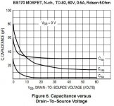
Bs170 60pF is the input capacitance - when VDS is zero volts.
https://www.onsemi.com/pub/Collateral/BS170-D.PDF
When VDS is about 5-60V capacitance is about 35-30pF.
But here is another more complicated capacitance. It is output capacitance, it changes from 80pF to 17pF depending on VDS. And even more it has a Miller Effect, when gain is 20x, capacitance will be 1600 pF - 340 pF plus input capacitance 60...30pF.
It limits open loop gain at high frequencies and distortion at that frequencies will rise accordingly.
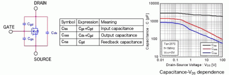
It's true that the effective input capacitance seen on the gate is multiplied by the gain of mentioned gain stage, but I think you looked at wrong figures in the datasheet, it is not Ciss but rather Crss (reverse capacitance) that should be taken into account and multiplied by the gain when finding out the effective input capacitance.
Unfortunately the datasheet doesn't have any figures for Crss, but we can extrapolate from the curves where we can see it is 30pF at Vds 0V and quickly falling below 5pF at Vds 10V.
For moderate listening levels the input capacitance is rather negligible and linear.
Of course, one little interesting experiment to perform is adding a cascode BJT on top of the BS170, if we want, but on the expense of a bit loss of rail-to-rail efficiency, but is that important for a "simple amplifier", I would say let us just enjoy the music.
")
Attachments
Last edited:
Hi. Thank You for correction, I have looked at the wrong figure. I have attached the file, here are schematically shown and explained these capacitances.but I think you looked at wrong figures in the datasheet, it is not Ciss but rather Crss (reverse capacitance) that should be taken into account and multiplied by the gain when finding out the effective input capacitance.
Attachments
Hi
This circuit is the original Lin but with mosfet outputs and an active load for Q1. Input impedance is 10k as the base of the input device is essentially a virtual-earth node.
Simple and safe for speakers, as another has pointed out. Not very efficient use of the PSU, though, as single-rail amps need a PT twice the size of a a split-rail amp for the same output power.
Hi, thank You for interest!
Could You explain what do You mean writing about:
Could You explain what do You mean writing about:
Not very efficient use of the PSU, though, as single-rail amps need a PT twice the size of a a split-rail amp for the same output power.
Hi
In a split-rail amp for say a 20W amp, the whole VA rating of the PT is available on an instantaneous basis from either half of the secondary. For each half of the wave, only one rail is loaded so only half the PT is loaded and the PT can be 20VA for the 20W amp.
On a single rail with capacitive output like your amp, the peak current must be pulled from the whole secondary, so the VA ratnig for the PT must be higher in this case.
If you look at historic amp designs, the PT went down with the transition to split rails.Where the cap provides protection against DC in the speaker, you pay the price with a bigger PT.
Hi, thank You for explanation. I want to correct You if You do not mind?
The biggest current flows from +E to gnd through transistors and load.
In both cases it is the same. For example we have dual rail with +-25VDC, and the same amp with single rail +50VDC.
In single rail version Load gets theoretically maximum 25VAC amplitude, because output is balanced at midpoint 25VDC and could swing only from 0 to 25V and from 25 to 50 V.
The same is in dual rail version. Output's midpoint is 0 V. Voltage could have theoretically maximum 25VAC amplitude. Current to the load is determinated by output voltage and load resistance, so if these parameters (voltage and load) ar the same in both cases - then same current flows through output transistors. If current and power is not wasted anywhere else it means that effectiveness of single rail and dual rail versions is about the same.
Some years ago ...
My suggestion:
Very important to get a clean, real sound is, not to use complementary devices - as complementary MosFets. Just one complementary stage and you have got "din", noise. Never a clean, clear tone.
Built up without a board. The result will be a MUCH cleaner, finer tone and better dynamic (quiet-loud/ piano-forte;-).
Just try it;-)
LG
Attachments
Hi
In a split-rail amp for say a 20W amp, the whole VA rating of the PT is available on an instantaneous basis from either half of the secondary. For each half of the wave, only one rail is loaded so only half the PT is loaded and the PT can be 20VA for the 20W amp.
guitar mod: You have ignored an important detail to make the scenarios equal - which they are not, as I've explained above.
Dear Nauta, in both cases PT average outcoming power raitings will be the same. I am not ingnoring Your details. Please take a closer look.
For instantaneous output power split rail could look less power hungry because each half is loaded alternately. For example if it is needed 1.58A of current to 8 Ohms load, the corresponding voltage would be 12.64 V . The losses in Vds and others not overlooked here for simplicity, just concentrating only to Power Supply power demands.
So, 12.64V multiplying by 1.58A = 20W. 20W to the load and 20W from power supply.
In single rail supply the voltage would be twice as big (12.64*2 = 25.28V) but current remains the same. So power demand from power supply from the first look is: 25.28V*1.58A = 40 W. Twice as big. But stop here. What happens in the negative cycle of the signal? It looks like no power demand is needed from power supply, because negative voltage rail is not -12.64V, but zero or GND. Power supply "rests" here. No current is flowing from Power supply, because upper half transistor is closed.
So instantaneous power demand looks better in split supply version, but average power demand and whole effectiveness are the same.
Last edited:
Hi mindutis,
No, C15 is compensation capacitor - for stability and for lower VAS impedance at High Frequencies because of the local negative feedback in schematic no2.
I ended with 18pF. Originaly it was 47pF.
Yes schematic No 2 is better, but not "bullet-proof stable" as the first one - without any compensation.
Further more for better stability it is good idea to have Zobel networks at the output of the amplifier (both versions) and also I recommend to use Zobel network just at the speaker cabinet terminals. (not shown in schematics as it should be obvious)
Some years ago ...
My suggestion:
Very important to get a clean, real sound is, not to use complementary devices - as complementary MosFets. Just one complementary stage and you have got "din", noise. Never a clean, clear tone.
Built up without a board. The result will be a MUCH cleaner, finer tone and better dynamic (quiet-loud/ piano-forte;-).
Just try it;-)
LG
Omitting the PCB will produce more messie sound imho
Hi
I don't see any purpose for R28.
The input base is biased by the divider, which then sets the output to the midpoint voltage. Gain is set by R17.27 and C9.
The nr2 topology is the same as Nelson et al did in the early 1960s as the next step to improve the Lin amp, by adding an input stage to separate the functions of error correction from bulk gain. Still stable and wide-bandwidth since the input and VAS are configured as what modern builders call a current-mode amplifier.
Thank You for suggestion, could You provide the schematic You are enjoying?Some years ago ...
My suggestion:
Very important to get a clean, real sound is, not to use complementary devices - as complementary MosFets. Just one complementary stage and you have got "din", noise. Never a clean, clear tone.
Just one complementary stage and you have got "din", noise. Never a clean, clear tone.
What does "din" mean?
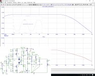
Here is my approach to the simplest symmetrical amplifier with LAT FETs and still single power rail. Middle voltage at the output is maintained when BJT drivers hfe are close. It could be some deviation, for example PNP hfe ~ 200 and NPN hfe ~ 300, then voltage at output would be around 1-1.5V from the middle point. But it is not big problem because output has no DC .
Completely stable with complex load, no compensation needed - as in the first version (simulated cable inductance and parasitic capacitance).
This one I could call "version 3". THD are similar to the first version. But now I prefer this
Clipping characteristics (here is shown 20kHz clipped sine wave) are also very good. No saturation, artifacts. R28 and R33 can be omitted (or reduced ten times) if power supply is well filtered. Then it would be about 10-6V more Peak to Peak Output voltage.
. Completely stable with complex load, no compensation needed - as in the first version (simulated cable inductance and parasitic capacitance).
This one I could call "version 3". THD are similar to the first version. But now I prefer this
Clipping characteristics (here is shown 20kHz clipped sine wave) are also very good. No saturation, artifacts. R28 and R33 can be omitted (or reduced ten times) if power supply is well filtered. Then it would be about 10-6V more Peak to Peak Output voltage.
Attachments
Pay attention that this schematic has very poor PSRR. Even more - if no measures are taken it will amplify PSU noise.
With typical PSU (Rectifier and 10 000 - 40 000 uF capacitor's per channel) optimal results would be, when VAS transistors power supply is decoupled via RC filter lets say 20-50 Ohms and 4700-10000uF.
(in schematic R33 should be omitted, R28 = 20-50 Ohms, C9 = 4700-10000uF).
With typical PSU (Rectifier and 10 000 - 40 000 uF capacitor's per channel) optimal results would be, when VAS transistors power supply is decoupled via RC filter lets say 20-50 Ohms and 4700-10000uF.
(in schematic R33 should be omitted, R28 = 20-50 Ohms, C9 = 4700-10000uF).
Last edited:
I’m interested in this amp and the first version for a point-to-point build. Can you provide a schematic that is complete and well labelled for us less technically gifted types that could be easily understood for a p-to-p build. Details of pssr avoidance being important here.
Thank you.
Thank you.
- Status
- This old topic is closed. If you want to reopen this topic, contact a moderator using the "Report Post" button.
- Home
- Amplifiers
- Solid State
- Very simple and very stable power AMP