Ranchu
Slowley but I am working too
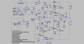
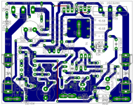
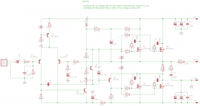
I have made another two boards.
First one very similar to previous one but DC servo added (hope correct way). For me it would be easier to add few zeners and extra OP-amp on the board.
The zener+diode network for nicer clipp can be adjusted a bit depending on the load If you make it clip nice symetric on 8R load than on 4R load positive rail will clip a bit lower tan negative side BJT cause bigger Vgs is eated by mosfet for load current demand.
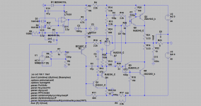
The second board I have made with CFP-BJT on both sides (just for fun), and in sim's it is showing very good performace, even with 1uF in parallel with 8R load.
Now somethink I do not understand very well. The nice R10=68kR resistor on Ranchu's schematic (from active VAS to neg-input).
If it is added this way it is reducing loop-gain quite a lot but it is reducing the THD too.
If I load the VAS to GND instead of NFB network than THD is not going down so much but is staying at the same (0,02% level) threw all audio frequency range (nice H2 H3 ratio from the bottom to 20kHz). Prapobly the best would be to do some listening tests (I do not remember if I had VAS load resistor in my previous board).
I have tryed also replacing the single tranistor input with CFP input with very good resaults. (it can be soldered in ''spider way'' and inserted instead single transistor easly).
Thanks too all !!!
Slowley but I am working too
I have made another two boards.
First one very similar to previous one but DC servo added (hope correct way). For me it would be easier to add few zeners and extra OP-amp on the board.
The zener+diode network for nicer clipp can be adjusted a bit depending on the load If you make it clip nice symetric on 8R load than on 4R load positive rail will clip a bit lower tan negative side BJT cause bigger Vgs is eated by mosfet for load current demand.
The second board I have made with CFP-BJT on both sides (just for fun), and in sim's it is showing very good performace, even with 1uF in parallel with 8R load.
Now somethink I do not understand very well. The nice R10=68kR resistor on Ranchu's schematic (from active VAS to neg-input).
If it is added this way it is reducing loop-gain quite a lot but it is reducing the THD too.
If I load the VAS to GND instead of NFB network than THD is not going down so much but is staying at the same (0,02% level) threw all audio frequency range (nice H2 H3 ratio from the bottom to 20kHz). Prapobly the best would be to do some listening tests (I do not remember if I had VAS load resistor in my previous board).
I have tryed also replacing the single tranistor input with CFP input with very good resaults. (it can be soldered in ''spider way'' and inserted instead single transistor easly).
Thanks too all !!!
Attachments
Last edited:
Hi borys
Great to see that you are still with us. I like your DC servo; even if it does add some complexity to gives peace of mind that the offset will be rock solid.
I see you have added an emitter resistor to the CFP VAS. Did you find this had some improvement?
R10 in my schematic (R28 in yours) controls the amount of nested feedback which reduces the amount of feedback around the output stage but helps linearise the VAS. Increasing or decreasing the amount of nested feedback will subtly change the distortion profile and is one of the tricks used to "voice" the amplifier.
I have added the VAS emiter resistor to reduce gain a bit, am was oscyllating with capactive loads without it. PLease take a look at the Nad 310 , 302 , 3020, all of them they have VAS resistor (prapobly for the same reason).
The VAS load resistor is a very nice trick not only performance-wise but soundwise too.
In my last hybrid it helped to make top octave more pleasend in sound (less harsh) and overal sound becamo more towards warm tones.
I was playing with your ''animal'' for a good few weaks and foud that it really needs fine tune with sound test more than measurements.
Some of my config was sounnding absolutley fine but only small change in circuit make it very hard to liten to it (top octave was very rough, even if measurements were fine).
What I like is almost ''audiophile'' harmonics balance (H2-H3-H4-ect).
Good job Ranchu !!
Last edited:
JLH found that overshoot on squarewaves correlated with poor sound quality........................I was playing with your ''animal'' for a good few weaks and foud that it really needs fine tune with sound test more than measurements.
Some of my config was sounnding absolutley fine but only small change in circuit make it very hard to liten to it (top octave was very rough, even if measurements were fine).
What I like is almost ''audiophile'' harmonics balance (H2-H3-H4-ect).............
He described in a couple of his Power Amplifier Design Build articles, the tuning of the feedback with an R+C, where the C was selected and then "tuned" with a VR to get best "shape" of the squarewave "corner" without overshoot. He claimed this gave best sound quality.
I have tried similar to this on many of my builds, but not quite in the JLH way, to remove overshoot from the test sq wave. This seems to me to give a correlation between sound quality and sqw testing.
Have you done anything similar?
Have you eliminated overshoot on fast signals?
For fast signals the RF attenuator on the input needs to be crippled. I change from 680ns to 68ns to allow the rise time of the sqw ramps to be ten times faster than worst case audio signals+interference.
Last edited:
AndrewT
Thanks for info.
Yes I have adjusted square waves with no overshoot. I have had only problem with bootstrap - had to add 2.2kR resistor to get correct sine waves at high amplitudes.
I will solder the new board and try to play with it a bit.
thimios
Hybrid is almost finished, just have to solder second channel and bring home. The bass is sorted (I have buffered VAS stage + added some load resistors to it and it is perfect now, will post some more info later on).
Regards
I'm waiting for improvementsAndrewT
Thanks for info.
Yes I have adjusted square waves with no overshoot. I have had only problem with bootstrap - had to add 2.2kR resistor to get correct sine waves at high amplitudes.
I will solder the new board and try to play with it a bit.
thimios
Hybrid is almost finished, just have to solder second channel and bring home. The bass is sorted (I have buffered VAS stage + added some load resistors to it and it is perfect now, will post some more info later on).
Regards
I would go for schematic from post 166, if ilimzn, AKSA and others would help to optimize and finish it.
As far as I am concerned, you can consider it 'public domain'. It does need a few refinements like a zener clamp for the MOSFET gates, and optimize the gate stoppers. Keep in mind that when the zener clamp for the bottom MOSFET clamps, the zener current goes right through the driver, so there is a current spike through the driver. It is recomended that the zener be on the gate side of the gate stopper so the current is limited.
The Vbe multiplier should work fine if attached to the BJT driver of the bottom MOSFET. However, it needs a bypass capacitor.
Ranchu
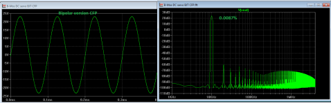
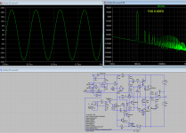
Sorry for spamming but it may look a bit interesting.
If someone would like can play with *.asc file atatched bellow.
Looks like CFP input is doing very good job. Harmonics balance looks nice too.
Regards
Peter
Sorry for spamming but it may look a bit interesting.
If someone would like can play with *.asc file atatched bellow.
Looks like CFP input is doing very good job. Harmonics balance looks nice too.
Regards
Peter
Attachments
AKSA
Thanks.
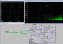
I went a bit further and I am going to do CFP-madness amp
I will solder it together and see if it will not blow up. Looks like cfp input pair is helping a lot at the higher frequeces.
The compensation - Miller one is not so required, looks that VAS to NFB 100pF is doing the job well.
Regards
Thanks.
I went a bit further and I am going to do CFP-madness amp
I will solder it together and see if it will not blow up. Looks like cfp input pair is helping a lot at the higher frequeces.
The compensation - Miller one is not so required, looks that VAS to NFB 100pF is doing the job well.
Regards
Attachments
Borys,
I will be very interested to hear what you think about a CFP in place of the singleton input device.
I tried it with simulation; didn't like it, BUT, the reality might be different. The 3K3 you choose for R20 is very important, as you know. And keep the slave device current a high current, say 2mA or even 3mA, so that you take advantage of the drive and linearity.
Good luck,
Hugh
Hi!
How much power would have the post 166 and 171 circuit?
Greets:
Tyimo
How much would you like?
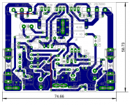
I've offered to do a layout for #166, which I'm working on now. Perhaps someone else might do one for #171 as well?
My plan is to make this flexible with an option for either one or two pairs output transistors, designed for 30V to 60V rails. The IRF240 devices are pretty rugged so 150W /8R should be within easy reach with 60V rails.
I might add an LTP active current source to Ilimzn's basic design, fixing the current over a wide voltage range so that only the VAS bootstrap resistors will necessitate adjustment to suit the target rail voltage.
What do you think this is a reasonable plan?
Something like this - not by far optimized, transistor types are representative (i.e BC640=BD139 in a different package), needs some refinement like gate protection, capacitor across Vbe multiplier, etc. - more of a doodle to show the idea:
Hi Ilimzn, is this the sort of thing you had in mind? I have added gate-drain zobels to each of the outputs (fc ~16MHz) to improve stability with some devices. I adopted this technique in a previous design and it worked beautifully; even with relatively small gate stoppers the MOSFETs were rock solid without the slightest hint of oscillation.
Degenerate the LTP or leave it as is?
Attachments
- Home
- Amplifiers
- Solid State
- Very simple quasi complimentary MOSFET amplifier