Hi Bhjazz, you’re right ") I’m using the balanced input board together with the balanced output board. At this moment the PBA2604 is in place making everything function. To use BA2018 I need to remove two awful tiny smd resistors. That’s a bit of a barrier for me.
I’m using the balanced input board together with the balanced output board. At this moment the PBA2604 is in place making everything function. To use BA2018 I need to remove two awful tiny smd resistors. That’s a bit of a barrier for me.
I’m also using Academy Audio’s power supply and just received a usb powerbank which is powering the whole “pre amp”. This seems to improve the soundstage which is really nice!
I’m using the balanced input board together with the balanced output board. At this moment the PBA2604 is in place making everything function. To use BA2018 I need to remove two awful tiny smd resistors. That’s a bit of a barrier for me. I’m also using Academy Audio’s power supply and just received a usb powerbank which is powering the whole “pre amp”. This seems to improve the soundstage which is really nice!
Hi,
Well, I am one of the believers re caps bypassing and if you came across one of my numerous tweeks here you are probably aware I do already use CD940 quite a lot. I have also carried some experiments, adding them in a row in the signal path and couldn't notice any difference with and without so for me, unless a colouration is wanted with boutique caps, that is the highest point re caps quality. But that's just me...
Probably as you I am very pleased with CD940 bypassing other caps, even film ones (polyester mainly). Of course very pleased also using them where I can.... directly.
I fail though to understand your reasoning, unless you want a special sound cooking with caps. Bypassing a Jantzen cap with CD940 would imply the latter is of better quality. I don't know if that's the case, never tried Jantzen, but my bet is they are probably very very similar. Anyway, rather than purchasing an expensive Jantzen, why aren't you directly going for a high qualitative CD940 1,8uF cap?
For sure the best possible and cheapest option in my eyes, unless space (not really here) or else is a constraint (tolerance perhaps... well, then you wouldn't consider adding a 0.1uF cap...)?
So CD940 1.8uF directly for me, 7$, that's what I would do, but that's just me
I hope this helps
Claude
At this moment the PBA2604 is in place making everything function. To use BA2018 I need to remove two awful tiny smd resistors. That’s a bit of a barrier for me.
So I was thinking about your post. First, what is the PBA2604? Is this where the SMD resistors are?
Thanks - it all makes sense now!
If you have a solder iron and a steady hand then removing them is straightforward. Check out this technique:
And I do understand that hitting something else on the board with a hot iron is possible. Still, you'll be able to implement your BA2018 with the Muses board. Work slowly and carefully. In fact, you might be able to get much of the solder up with solder wick to being with.
If you have a solder iron and a steady hand then removing them is straightforward. Check out this technique:
Work slowly and carefully. In fact, you might be able to get much of the solder up with solder wick to being with.Hi you all,
The boards arrived last week, and so today I started assembling.
Now there is a note on the guide: ¨Please note that the PCB shown stuffed is setup for using the “big” output transistors, where R11,12, 32, 33 are 15ohm, and R23, 46 are omitted.¨
Well, at R11,12, 32, 33 I soldered the 27R and at R23 and 46 I put in the 330R. Is this correct?


Safety gnd has nothing to do with it, irrelevant.
Before anything else, check continuity between all jfet legs and the next point in the circuit (meaning a total of 12 measurements with dmm set to ohms). You want readings of about 0 ohms. Push the jfets slightly to dee if the measurements change (a bad sign).
Then please post even more pics, and verify that all the bipolar transistors are the correct type in the correct location with correct orientation, and also double check diode orientation. The diodes are part of the biasing circuit.
Also, please measure and post voltage drops across all the 10 ohm resistors in conjuction with the JFETs (dmm set to mV, one probe at each leg of the resistor).
Then, measure voltage drop across bias resistor.
Post results.
This circuit can be a real biatch, and jfet issues is the most common. And not to be impolite, but you - like most of us - could use some training in smd soldering - the most difficult part of the job in this case.
Last edited:
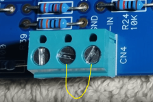
I have a question: both power and audio in have 3 connections, a +/-/ground. I only have 2 wires each for right and left audio and power? 🤷♂️
What are you using as a power supply? The power supply needs to be bipolar, with a V+, Ground, and V- output. Provide a picture of your power supply. Also provide a picture of your setup of power supply and preamp board showing all connections.
What do you mean by continuity between all jfet legs? Measure between the 3 legs which should be 0 ohms?Safety gnd has nothing to do with it, irrelevant.
Before anything else, check continuity between all jfet legs and the next point in the circuit (meaning a total of 12 measurements with dmm set to ohms). You want readings of about 0 ohms. Push the jfets slightly to dee if the measurements change (a bad sign).
Then please post even more pics, and verify that all the bipolar transistors are the correct type in the correct location with correct orientation, and also double check diode orientation. The diodes are part of the biasing circuit.
Also, please measure and post voltage drops across all the 10 ohm resistors in conjuction with the JFETs (dmm set to mV, one probe at each leg of the resistor).
Then, measure voltage drop across bias resistor.
Post results.
This circuit can be a real biatch, and jfet issues is the most common. And not to be impolite, but you - like most of us - could use some training in smd soldering - the most difficult part of the job in this case.
- Home
- Amplifiers
- Pass Labs
- Wayne's BA 2018 linestage