

Discrete OpAmp - Replaces Dual Channel DIP8 - design and PCB
Posted 11th May 2017 at 06:28 PM by googlyone
Well here I am travelling again, and this time stuck for an extra week away from home. The design bug has bit, and this time I tried keeping things small rather than crazy.
I have built a number of discrete operational amplifiers in the past. Usually integrating everything onto the board so that they wind up being preamplifiers rather than operational amplifiers.
If that confuses you - the difference is that an operational amplifier needs to be plugged into a circuit to be useful, a preamp is a standalone PCB.
The inspiration was seeing a burson amp on ebay. I looked and thought to myself "I keep starting that, and keep ending up with a preamp". Then I thought "Do it right for once".
The resultant goals:
- Dual channel op amp
- DIP8 pinout
- Good perfromance
- Class A (vs class AB which many are)
- Minimum size, whilst
- Sticking to 0805 SMD resistors caps, and
- Reasonably available transistors.
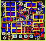
The result is rather unassuming, two PCBs each of which sits above the rows 1-4 and 5-8 of the DIP8:
and
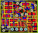
To give you an idea of the scale of things, these boards are 0.86 inches wide and 0.78 inches tall. So just over 0.66 square inches.
I could have pushed for smaller but that would have required me to pull some bits off, and that was not a compromise that I was willing to make in this version.
The schematics are below:
Schematic CH1.pdf
and for the second channel an unsurprisingly similar schematic:
Schematic CH2.pdf
Things to note:
- The input differential pair is a dual transistor. This gives me comfort knowing that the input pair are the same temp, and probably from the same batch. I have used these before with great success.
- The input diff pair has a current source - again a dual to save space.
- The input diff pair has a current mirror load. There are more bits to this, but this does force the input diff pair to run at equal currents in each arm, and if you are from the more scientific school of design will be better than a simple resistor in terms of distortion.
Some of the resistance values around the input stage are subject to optimisation. If I ever do that.
The input stage has a buffer before a pretty conventional VAS. Both of these are BC858, which are bog standard SMT BJT's. I bet you can find a dozen equivalents, many of which you prefer.
The Schematic shows 180pF Miller cap. I am quite sure this can be an awful lot less, and once I build some real ones, I will put a better value in there. I would probably start with 33 or 68pF. Mainly because I have a reel of each of these
That odd looking 1N4148 diode in there is purely to stop the Vas from misbehaving during clipping. The input diff pair will "mang against the negative rail" and drive a LOT of current into the buffer and subsequently the Vas. The diode redirects this current to the output drive and makes things all bahave so much better than without.
I have shared the voltage reference of the diff pair current source with the VAS current source and also the output stage(s).
Huh? Output stages? I'll get to that....
The Vas is a BC846 or any SOT223 NPN device. I kind of imagine I will be using BC849 as I have lots of these.
The output stage is class A. As is everything else. I started with one pair of transistors, and to be honest will start by loading one pair.
I added the option for a second pair to allow doubling of the CLASS A current. The reason for this is that the output stage runs at 6mA in each of the two devices. With one set of devices, 6mA will allow 6V into 1k Ohms.
With a second pair this allows 12V into 1K, which is in my mind more than enough.
The choice of 6mA per pair is to ensure that if the output is shorted, everything is OK and nothing will be over stressed. (I have assumed +/- 15Volt rails, which is a reasonable limit and that which the use of BC849 devices allows).
the reason I used Class A is that this should avoid crossover distortion.
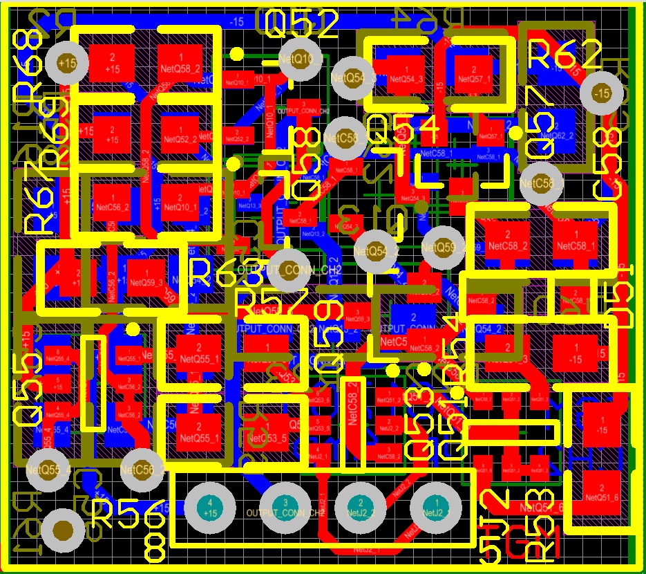
The final boards look like the following for all the layers....
Final Artwork CH1.pdf
and
Final Artwork CH2.pdf
I am getting 50 of each board made up. Damn I hope I didn't mess anything up!
If you want some to play with, drop me a line! I will never make 50 of these and will happily post you a couple to play with.
Similarly, next time I am not running for a plane (they are calling groups right now) I will upload the ALTIUM file.
If you have any improvements / tweaks, again drop me a line.
I have built a number of discrete operational amplifiers in the past. Usually integrating everything onto the board so that they wind up being preamplifiers rather than operational amplifiers.
If that confuses you - the difference is that an operational amplifier needs to be plugged into a circuit to be useful, a preamp is a standalone PCB.
The inspiration was seeing a burson amp on ebay. I looked and thought to myself "I keep starting that, and keep ending up with a preamp". Then I thought "Do it right for once".
The resultant goals:
- Dual channel op amp
- DIP8 pinout
- Good perfromance
- Class A (vs class AB which many are)
- Minimum size, whilst
- Sticking to 0805 SMD resistors caps, and
- Reasonably available transistors.
The result is rather unassuming, two PCBs each of which sits above the rows 1-4 and 5-8 of the DIP8:

and
To give you an idea of the scale of things, these boards are 0.86 inches wide and 0.78 inches tall. So just over 0.66 square inches.
I could have pushed for smaller but that would have required me to pull some bits off, and that was not a compromise that I was willing to make in this version.
The schematics are below:
Schematic CH1.pdf
and for the second channel an unsurprisingly similar schematic:
Schematic CH2.pdf
Things to note:
- The input differential pair is a dual transistor. This gives me comfort knowing that the input pair are the same temp, and probably from the same batch. I have used these before with great success.
- The input diff pair has a current source - again a dual to save space.
- The input diff pair has a current mirror load. There are more bits to this, but this does force the input diff pair to run at equal currents in each arm, and if you are from the more scientific school of design will be better than a simple resistor in terms of distortion.
Some of the resistance values around the input stage are subject to optimisation. If I ever do that.
The input stage has a buffer before a pretty conventional VAS. Both of these are BC858, which are bog standard SMT BJT's. I bet you can find a dozen equivalents, many of which you prefer.
The Schematic shows 180pF Miller cap. I am quite sure this can be an awful lot less, and once I build some real ones, I will put a better value in there. I would probably start with 33 or 68pF. Mainly because I have a reel of each of these
That odd looking 1N4148 diode in there is purely to stop the Vas from misbehaving during clipping. The input diff pair will "mang against the negative rail" and drive a LOT of current into the buffer and subsequently the Vas. The diode redirects this current to the output drive and makes things all bahave so much better than without.
I have shared the voltage reference of the diff pair current source with the VAS current source and also the output stage(s).
Huh? Output stages? I'll get to that....
The Vas is a BC846 or any SOT223 NPN device. I kind of imagine I will be using BC849 as I have lots of these.
The output stage is class A. As is everything else. I started with one pair of transistors, and to be honest will start by loading one pair.
I added the option for a second pair to allow doubling of the CLASS A current. The reason for this is that the output stage runs at 6mA in each of the two devices. With one set of devices, 6mA will allow 6V into 1k Ohms.
With a second pair this allows 12V into 1K, which is in my mind more than enough.
The choice of 6mA per pair is to ensure that if the output is shorted, everything is OK and nothing will be over stressed. (I have assumed +/- 15Volt rails, which is a reasonable limit and that which the use of BC849 devices allows).
the reason I used Class A is that this should avoid crossover distortion.
The final boards look like the following for all the layers....
Final Artwork CH1.pdf
and
Final Artwork CH2.pdf
I am getting 50 of each board made up. Damn I hope I didn't mess anything up!
If you want some to play with, drop me a line! I will never make 50 of these and will happily post you a couple to play with.
Similarly, next time I am not running for a plane (they are calling groups right now) I will upload the ALTIUM file.
If you have any improvements / tweaks, again drop me a line.
Total Comments 0


