... start tuning for lowest SNR with homebrew h-field probe ... need to add some cnc machined mu-metal.
SNR from lab is as low as 125 (A-weighted)
Current SNR is about 110 db (A-weighted)
Something to compare against? ATI AT6005 Amplifier | Sound & Vision
Really nice parts using CFA technology with aboutSomething to compare against? ATI AT6005 Amplifier | Sound & Vision
- 0.03% THD 20Hz-20kHz@300W@8R (bw?)
- SNR 128db referenced to 300W@8R
SA2014 using VFA technology has due to some small hum currently
- max. 0.0022 % THD+N 20kHz@200W@8R. (bw 80kHz)
- max. 0.0012 % THD+N 20Hz-10kHz@200W@8R (bw 80kHz)
- SNR 110db (A-w) referenced to 200W@8R
Bring it on Toni! I'm just learning - I sure wish I had your skill. FYI more specs on the ATI amp here AT6000 Stereo Amplifier
SA2014 - revisited schematics - bill of materials
... finalized schematics and bill of material...
Note: Schematics and BOM are free to use only for non commercial DIY projects.
WARNING: these circuits are using and providing very high AC and DC voltages and are therefore very dangerous and can be lethal. I am not responsible for any costs, damage and/or injury using these schematics and BOM. Do not use this schematics if you do not have the necessary experience and knowledge.
All BOM values have been carefully checked - if you detect errors please PM me.
Amplifiers name has been set to SA2014 but unfortunately most files are containing the old name SA2013.
Have Fun, Toni
Attachments
-
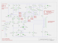 sa2013_input_vas_stage_schematic.png273.7 KB · Views: 3,767
 -
sa2013_input_vas_stage_schematic.pdf19.3 KB · Views: 865
-
sa2014_bom.pdf58.2 KB · Views: 871
-
sa2013_power_supply_schematic.pdf13.9 KB · Views: 706
-
sa2013_bias_output_stage_schematic.pdf29 KB · Views: 774
-
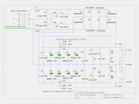 sa2013_power_supply_schematic.png171 KB · Views: 3,619
 -
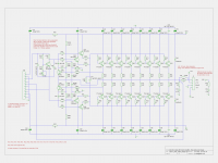 sa2013_bias_output_stage_schematic.png182.8 KB · Views: 3,729
Last edited:
... finalized schematics...
Hi Toni
Can you post a finalized ASC too?
I want to run a few more comparisons.
Best wishes
David
Hi Toni
Can you post a finalized ASC too?
I want to run a few more comparisons.
Best wishes
David
Voila: must be post #925
BR, Toni
Hi Toni
Can you post a finalized ASC too?
I want to run a few more comparisons.
Best wishes
David
Attached all simulation files together. Only Cordell-Models.txt has to be downloaded from Bob's homepage.
Attachments
Attached all simulation files...
Thanks for that, I did a simulation of the inner loop Return Ratio, at the VAS input.
Have you looked at this, in particular the PM?
Best wishes
David
Thanks for that, I did a simulation of the inner loop Return Ratio, at the VAS input.
Have you looked at this, in particular the PM?
Best wishes
David
Dear David,
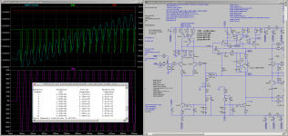
don't know if I understand you correctly. Do you mean a measurement like the attached picture?
Attachments
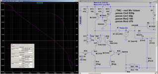
Almost. I meant at point VAS-INP.Do you mean a measurement like the attached picture?
This then includes the effect of the feedback via the TMC network.
There are two feedback paths into the VAS (transistor Q6 base) and you need to probe the total to determine stability.
It can be helpful to study the path you have probed, to determine its contribution, but it does not show the true stability.
The true stability, unfortunately, is often less than one would expect, based on just one path.
Best wishes
David
Last edited:
A couple remarks:
Is the R18 really needed? R19||R221||R22 is about 220Ohm, so what difference makes another 47?
When this amp is going to clipping, D1-D2 get shorted through R24,R27 and Q11 BE, which may lower LTP current (after some time needed to discharge C6). This may be harmless, but ...
Q11 base should be powered through separate resistor from R14-R17 common point, and better stabilized with additional transistor (more thermal stable). Look at "Honey Badger" for example.
A couple remarks:
Is the R18 really needed? R19||R221||R22 is about 220Ohm, so what difference makes another 47?
...
to which schematic do you refer?
Does that mean insert Tian probe into the line...
Also means...
Yes and yes.
Best wishes
David
to which schematic do you refer?
To latest one, input/VAS stage. Sorry for confusion.
A couple remarks:
Is the R18 really needed? R19||R221||R22 is about 220Ohm, so what difference makes another 47?
When this amp is going to clipping, D1-D2 get shorted through R24,R27 and Q11 BE, which may lower LTP current (after some time needed to discharge C6). This may be harmless, but ...
Q11 base should be powered through separate resistor from R14-R17 common point, and better stabilized with additional transistor (more thermal stable). Look at "Honey Badger" for example.
Think you are referring to attached schematic...
R6+R18 as near as possible at bases of LTP bjt are for paranoid safety against HF. BC550C are fT 250-300Mhz devices.
R21+R22 (equivalent to 8.2k) is to reduce thermal induced distortion when driving high output levels.
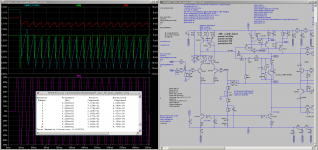
You are right that clipping "kills" LTP current. Attached a simulation of this case driving a 60Hz bass wave heavy overloaded. Funny: The distortion level during clipping is lower using the single ccs power supply.
But if it starts clipping its too late. Can't hear the difference between 9.10% and 9.15% distortion.
")
As always - many thanks for reporting.
Toni
Attachments

Last edited:
Have you observed the BC5xxC to oscillate, in a situation where the 47R base stoppers were the solution?
Fairchild BC5xxC (rather than OnSemi/Motorola for instance) have much less transconductance at RF, so may be less prone to parasitic oscillation, if they are prone to it at all with normal layout practices.
Fairchild BC5xxC (rather than OnSemi/Motorola for instance) have much less transconductance at RF, so may be less prone to parasitic oscillation, if they are prone to it at all with normal layout practices.
Have you observed the BC5xxC to oscillate, in a situation where the 47R base stoppers were the solution?
Fairchild BC5xxC (rather than OnSemi/Motorola for instance) have much less transconductance at RF, so may be less prone to parasitic oscillation, if they are prone to it at all with normal layout practices.
Thanks for info! Can't remember exactly, have no screen shots, but during development of the MyDOA (see first post of this thread for an index) I've had more stability and better square wave response adding those 47R at the LTP bases when driving the opamp on breadboard and unshielded.
Haven't tested Fairchild BC550C in SA2014 ips/vas but some MyDOAs are running perfect using Fairchild BC550C.
- Home
- Amplifiers
- Solid State
- 2stageEF high performance class AB power amp / 200W8R / 400W4R