2stageEF 50W MOSFET - aka SA2015MT
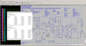
Simulation only: 50W/8R MOSFET amplifier for mid and treble in a 3 channel active crossover power amplifier:
BR, Toni
Simulation only: 50W/8R MOSFET amplifier for mid and treble in a 3 channel active crossover power amplifier:
- combined TMC/Cherry compensation
- using 2x30V AC for supply
- THD20k@50W@8R: 0.0003 %
- overall PM 80, GM16
BR, Toni
Attachments
Simulation only: 50W/8R MOSFET amplifier for mid and treble in a 3 channel active crossover power amplifier:
- combined TMC/Cherry compensation
- using 2x30V AC for supply
- THD20k@50W@8R: 0.0003 %
- overall PM 80, GM16
Hi Toni
Nice to see you continue to work on this, all I have done recently is mathematics, not quite real, even if it pays real money.
How do you plan to handle the crossover?
I plan to implement it as part of the amplifier, just like a power op-amp.
A bit less flexible of course, will probably use DSP to find the frequency response then build that curve into the amp.
Best wishes
David
Simulation only: 50W/8R MOSFET amplifier for mid and treble in a 3 channel active crossover power amplifier:
Simulation shows good and stable results but will it work on breadboard?
- combined TMC/Cherry compensation
- using 2x30V AC for supply
- THD20k@50W@8R: 0.0003 %
- overall PM 80, GM16
BR, Toni
Hi Toni,
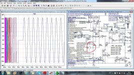
Nice to have you back here, very nice amp. I suggest you to bootstrapped the cascode biasing instead referenced to the ground, and you can have some THD improvement (Q19 on the attached picture). By the way I think that you need to increase the zener (D6) current to pass the knee.
BR Damir
Attachments
Hi Toni
...
How do you plan to handle the crossover?
...
Dear Dave,
the plan is to use an analog 3 channel LR24 with time delay blocks to split the input signal into 3 blocks. (for crossover have a look at Rane Corporation)
Bass speaker will get the 200W 2StageEF amp.
Mid speaker will get a 50W 2StageEF MOSFET amp.
Treble speaker will get a 50W 2StageEF MOSFET amp.
A tower case which contains the 3 amplifiers + active crossover will be placed directly left or right at the speaker.
My Denon AVR-X7200W will handle the DSP part if needed.
BR, Toni
Hi Toni,
Nice to have you back here, very nice amp. I suggest you to bootstrapped the cascode biasing instead referenced to the ground, and you can have some THD improvement (Q19 on the attached picture). By the way I think that you need to increase the zener (D6) current to pass the knee.
BR Damir
Thx for the hints and the nice words!
Have incorporated your recommendations. Attached the corrected version.
BR, Toni
Attachments
LTspice allows capacitors with value zero!
"Ctian" will be used for switching inputs to ground using 1kF cap during calculating "Tianprobe B".
BR, Toni
"Ctian" will be used for switching inputs to ground using 1kF cap during calculating "Tianprobe B".
BR, Toni
Attachments
LTspice allows capacitors with value zero!
I didn't know that. When I tried 0 value resistors I received errors so I never tried capacitors.
Is that new? Will try to check it today but my LTSpice machine is down, needs to be fixed first.
So I haven't had a chance to check your latest.
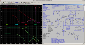
The ULGF is pushed pretty far up and PM is not conservative, to say the least. I assume you have checked this as the output transistors approach the rails. You think this is adequate?
Best wishes
David
...
The ULGF is pushed pretty far up and PM is not conservative, to say the least. I assume you have checked this as the output transistors approach the rails. You think this is adequate?
Best wishes
David
Dear David,
thanks for checking this. Any recommendations are always highly welcome. As it is a work in progress I have it pushed to the limits watching for instabilities (e.g. square wave overshoot, oscillation ...).
The initial question was
"... but will it work on breadboard?"
caused by the "not so good" cherry compensation test results during development of this threads amplifier. Maybe this combined compensation type will not work as expected.
My holidays will start in 9 days - hopefully I will find time building a prototype.
")
BR, Toni
The ULGF is pushed pretty far up and PM is not conservative, to say the least.
Phase margin of the global loop looks to be over 60°. This should be plenty, no?
The phase margin of the inner loop is much smaller, perhaps you are referring to this? In my experience it can be difficult to get the phase margin much bigger without severely compromising the global loop. I’ve never investigated the sensitivity of the inner loop to component and operating variations so I don’t know if one can get away with these small margins.
The initial question was "... but will it work on breadboard?"
caused by the "not so good" cherry compensation test results during development of this threads amplifier. Maybe this combined compensation type will not work as expected.
This type of combined compensation is difficult to analyse.
I will be very interested in your results to see how they compare to theory.
Phase margin of the global loop looks to be over 60°. This should be plenty, no?
Maybe. I was almost shocked to see how much PM was reduced once I included a bit of capacitance in the load and simulated near peak amplitude, to reduce the output transistor Vce.
That was in my own BJT test amp, Paul made similar comments after I recommended he try such tests on his similar, BJT amp.
Not sure how it will work out here.
Yes, the inner loop looks a bit scary to me....of the inner loop is much smaller... In my experience it can be difficult to get the phase margin much bigger without severely compromising the global loop. I’ve never investigated the sensitivity of the inner loop to component and operating variations so I don’t know if one can get away with these small margins.
40 MHz so parasitics will matter, and not much room for error.
Best wishes
David
PS I posted a little on the problem of simultaneous optimization of the two loops, not easy but possible.
Last edited:
A hint how to do this?...
Maybe. I was almost shocked to see how much PM was reduced once I included a bit of capacitance in the load and simulated near peak amplitude, to reduce the output transistor Vce.
...
...
PS I posted a little on the problem of simultaneous optimization of the two loops, not easy but possible.
Maybe you can add a link to this? Thx!
BR, Toni
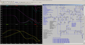
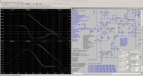
Added capacitive loads:
A1: 4.7nF || 8R
A2: 100nF || 8R
A3: 470nF || 8R
A4: 2µF || 8R
Could you clarify, as it is not visible in the screenshot - presumably the amplifier has a zobel (RC) on its output to ground, and then a series L (possibly with a parallel R) before the actual output terminal, and it is the actual output terminal at which these load networks are being connected?
A hint how to do this?
http://www.diyaudio.com/forums/soli...signed-during-lunch-breaks-2.html#post4178191
Second reply in the post.
http://www.diyaudio.com/forums/solid-state/261973-middlebrook-gft-probe.html#post4076143Maybe you can add a link to this? Thx!
I am pretty happy with this. I was able to land the phase peak square on top of the ULGF for both the inner and outer loop simultaneously.
Last edited:
http://www.diyaudio.com/forums/soli...signed-during-lunch-breaks-2.html#post4178191
Second reply in the post.
http://www.diyaudio.com/forums/solid-state/261973-middlebrook-gft-probe.html#post4076143
I am pretty happy with this. I was able to land the phase peak square on top of the ULGF for both the inner and outer loop simultaneously.
Many thx!
BR, Toni
Could you clarify, as it is not visible in the screenshot - presumably the amplifier has a zobel (RC) on its output to ground, and then a series L (possibly with a parallel R) before the actual output terminal, and it is the actual output terminal at which these load networks are being connected?
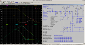
Attached after output zobel. Have a look at the previously attached asc file.
BR, Toni
Added capacitive loads:
Looks like the Zobel isolates the amp pretty well, just like it is intended to.
This was my experience also, I tried without a Zobel but the deterioration in stability was severe just to eliminate a few simple parts.
A Zobel is practically essential if you want robust stability.
Best wishes
David
Attached after output zobel. Have a look at the previously attached asc file.
Output Zobel is the R+C from output to ground.Looks like the Zobel isolates the amp pretty well, just like it is intended to.
The Thiele Network has both and R+C to ground and an L||R in series before the speaker terminals.
Are either of your referring to the L||R part of the Thiele Network?
- Home
- Amplifiers
- Solid State
- 2stageEF high performance class AB power amp / 200W8R / 400W4R