That’s what I used in my 2007 amp. Didn’t know it was Lender - I saw it in one of James Biorngino [sp?] amp designs from way back.
Do the Lender trick with the first stage to second stage connection. Voila, you get a push-pull VAS with well defined bias currents in both stages. You also get more gain than either resistor loads or folded cascode. (however less gain than a current mirror)
_
Do either of you know any references that explain how to design that circuit?
I was wondering about this in Bob's DH-220C presentation. He uses this configuration whenever there is no current mirror, but I couldn't find an explanation for the design in either Cordell's or Self's books.
The circuit on page 4 looks similar to the folded cascode circuit on page 10, but evidently the performance is very different. I would like to learn more.
The link in question:
http://forum.cxem.net/applications/core/interface/file/attachment.php?id=515698
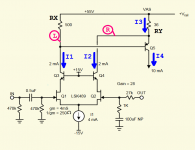
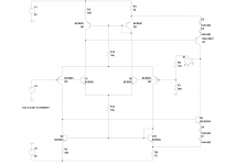
I've attached an image. Some things that the circuit designer will consider when proportioning this circuit, might include
* Choose I4, the current in the 2nd stage aka "VAS". It should be large, so the VAS can drive the OPS authoritatively. But not so large that the power dissipation of the VAS transistors is unacceptably high. Bob Cordell has chosen 10mA which, with plus and minus 55V supplies, means the VAS transistors will dissipate 0.55 watts. They need to be TO-126 devices and they need heatsinking.
* Choose I1 and I2, the currents in the two halves of the input stage differential pair. Choose them to give acceptable transconductance gm, while minimizing power dissipation in the input pair. Bob Cordell has chosen 2mA for each; Douglas Self very often chooses 3mA for each. That's 0.11W or 0.17W with 55V rails.
* Calculate the gm of input devices Q1 and Q2, using the hybrid pi model. Or from the semiconductor physics device equations. Or from curves on the manufacturer's datasheet.
* Choose resistor RX such that (gm_Q1 * RX) >= 2.0 . Then the half circuit gain (at node L) is 1.0 or greater. This ensures the input stage actually provides useful gain, it's not merely a current conveyer.
* Calculate the voltage at node L. It's Vtoprail - (I1 * RX). You now know Vtoprail, you know I1, you know Rx. So this is simple arithmetic.
* Calculate the voltage at node R. It's VL + VBE so again this is simple arithmetic
* Calculate I3. It's I4 - I2 and you know both, so it's simple arithmetic.
* Calculate RY. It's (Vtoprail - VR) / I3 . Again simple arithmetic
* Victory
The difficult bits are (A) estimating VBE to within 5 millivolts; and (B) calculating gm to within 5%. I recommend plain ordinary lab measurement. It's very difficult to disagree with measured data. Especially if you made the measurements yourself!
_
Attachments
How about this sort of thing been mentioned?
Hi,
By combining IPS I picked up from Edmond Stuart and another solution by someone else (not me but can't cite the person) this was the result. Not quite mirrors but these could be reinstated. It clips better with resistors...
Paul
Hi,
By combining IPS I picked up from Edmond Stuart and another solution by someone else (not me but can't cite the person) this was the result. Not quite mirrors but these could be reinstated. It clips better with resistors...
Paul
Attachments
Wow, medium power devices in TO-126 for the inputs, but low power TO-92s for the current source loads.
Yes, it's just an experiment at the moment. Could easily add cacodes and use TO-92 for the input devices. The TO-92 is fine for the "current mirror".
In it's current configuration from a dissipation point of view the choice of transistors makes sense. The rails for this are 63V in my sims. It was a quick cut, simplify and paste....
Paul
Last edited:
Some problems with the Cordell amplifier of figure 4.1
In Cordell’s amplifier of figure 4.1 on page 88 of the second edition of his book, he uses two diodes D3 and D4 in parallel opposition across the differential inputs of the input stage. Unfortunately, this is a terrible idea because these diodes prematurely and unnecessarily curtail the amplifier’s slew rate.
What is actually required are three-diode strings in parallel opposition across the differential inputs of the input stage, and these are mandatory because they prevent the base-emitter junctions of the input differential transistor pair, Q1 and Q2, from being destructively reverse-biased by unusually large input voltages. The temptation to use fewer than three diodes in series per string should be resisted for the aforementioned reason. Diodes D5 and D6 in parallel opposition and connected between the collectors of the input differential transistor pair, Q1 and Q2, are completely unnecessary.
On page 89, Cordell also says that capacitor C7 across the base-emitter junction of the buffer driving his input stage’s current mirror helps “reduce [the buffer’s] role at very high frequencies”. In fact, this capacitor eliminates the very pronounced peaking in the buffered current mirror’s frequency response and, therefore, eliminates the mirror’s potential for provoking instability, as the late, great Barry Gilbert pointed out in “Analogue IC Design: the Current Mode Approach”, pages 265-267, ISBN: 0863412971.
Crude , but I just use this ...
It's the most popular , too. (below)
Over 100 built by others. My 4 ... I used two for music.
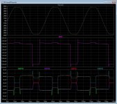
One I used for abuse , can I blow it ?? 0-70C VAS I(4.1-4.2mA).
Idle to full -same. Clip (below 2) VAS drops a little to 3.5mA.
The input stage became cool , in fact .... always cool.
Just a big 17mA per rail discrete op-amp with a little light show
LED's flicker on clip.
I can't understand the dislike of complimentary designs.
Or , using so much current in all the stages. I know I could get
more gain @ 2-3mA, but use 546B/556B (or C). All semi's are lower voltage
except Q12/13.
OS
It's the most popular , too. (below)
Over 100 built by others. My 4 ... I used two for music.
One I used for abuse , can I blow it ?? 0-70C VAS I(4.1-4.2mA).
Idle to full -same. Clip (below 2) VAS drops a little to 3.5mA.
The input stage became cool , in fact .... always cool.
Just a big 17mA per rail discrete op-amp with a little light show
LED's flicker on clip.
I can't understand the dislike of complimentary designs.
Or , using so much current in all the stages. I know I could get
more gain @ 2-3mA, but use 546B/556B (or C). All semi's are lower voltage
except Q12/13.
OS
Attachments
Not to complicated, but low distortion and high slew rate.
https://www.diyaudio.com/forums/solid-state/248105-slewmaster-cfa-vs-vfa-rumble-1054.html#post6461396
https://www.diyaudio.com/forums/solid-state/248105-slewmaster-cfa-vs-vfa-rumble-1054.html#post6461396
I've attached an image. Some things that the circuit designer will consider when proportioning this circuit, might include
* Choose I4, the current in the 2nd stage aka "VAS". It should be large, so the VAS can drive the OPS authoritatively. But not so large that the power dissipation of the VAS transistors is unacceptably high. Bob Cordell has chosen 10mA which, with plus and minus 55V supplies, means the VAS transistors will dissipate 0.55 watts. They need to be TO-126 devices and they need heatsinking.
* Choose I1 and I2, the currents in the two halves of the input stage differential pair. Choose them to give acceptable transconductance gm, while minimizing power dissipation in the input pair. Bob Cordell has chosen 2mA for each; Douglas Self very often chooses 3mA for each. That's 0.11W or 0.17W with 55V rails.
* Calculate the gm of input devices Q1 and Q2, using the hybrid pi model. Or from the semiconductor physics device equations. Or from curves on the manufacturer's datasheet.
* Choose resistor RX such that (gm_Q1 * RX) >= 2.0 . Then the half circuit gain (at node L) is 1.0 or greater. This ensures the input stage actually provides useful gain, it's not merely a current conveyer.
* Calculate the voltage at node L. It's Vtoprail - (I1 * RX). You now know Vtoprail, you know I1, you know Rx. So this is simple arithmetic.
* Calculate the voltage at node R. It's VL + VBE so again this is simple arithmetic
* Calculate I3. It's I4 - I2 and you know both, so it's simple arithmetic.
* Calculate RY. It's (Vtoprail - VR) / I3 . Again simple arithmetic
* Victory
The difficult bits are (A) estimating VBE to within 5 millivolts; and (B) calculating gm to within 5%. I recommend plain ordinary lab measurement. It's very difficult to disagree with measured data. Especially if you made the measurements yourself!
_
Wow, thank you Mark! This is so awesome!
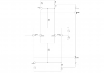
Further to my earlier post Resistor version regarding a solution to the undefined VAS current, I thought it would be a good idea to show the full current mirror version. Easier to follow. A CMCL is embedded within this at the cost of 4 diodes.
Paul
Paul
Attachments
That’s what I used in my 2007 amp. Didn’t know it was Lender - I saw it in one of James Biorngino [sp?] amp designs from way back.
Just checked and I used the Lender technique in the e-Amp from 2012 as well (180 W amp) - also no balance issues.
Klever Klipper - clip sharpness
I haven't seen any discussions on the "sharpness" of soft-clip not the effect on amplifier "sound".
My thinking is that the added onset distortion from a soft-clip circuit is not audible so it doesn't change the "sound" of an amplifier that has no "sound". So the added onset distortion from a soft-clip circuit is a non-issue in my opinion. See posts here
Further, my thinking is the earlier soft-clip is the less you hear the effect of adding the soft clip circuit once a clip occurs -- that might sound counter-intuitive, but when you consider starting later results in a sharper clip which generates higher-order harmonics than one starting earlier, then it can make some sense to start earlier.
Hi benb,I saw the Klever Klipper on the Neurochrome site (and poking around on diyaudio, this appears the most appropriate place to discuss it) and saw how the circuit begins distorting at a "relatively low" power level (distortion starts going up around a third of max power output) versus regular clipping. I'm thinking that two Schottky diodes with their lower forward voltage (and presumably sharper knee) might work better here. The BAT54S conveniently has two series diodes in one package.
Would Schottkys "sound better" here, or would the sharper knee make for a harsher sound when the distortion finally does kick in? Also, it seems one can adjust knee sharpness by adding diodes of either type in series.
Has the "sharpness" of such pre-power-amplifier limiters been discussed before, in this thread (sorry, I haven't read much here) or elsewhere?
I haven't seen any discussions on the "sharpness" of soft-clip not the effect on amplifier "sound".
My thinking is that the added onset distortion from a soft-clip circuit is not audible so it doesn't change the "sound" of an amplifier that has no "sound". So the added onset distortion from a soft-clip circuit is a non-issue in my opinion. See posts here
and my amps measured soft clip transfer curve is shown here.The soft clip option is usually rejected by designers aiming for ultra-low distortion because it adds distortion even at 10% of full power, so you no longer get ultra-low distortion up to full power.
But in practice with soft clipping you can have clipping more often before you hear clipping. So it is helpful if you don't want to change your loudspeakers OR you don't want a monster amp.
I believe if the soft clip is done right it doesn't add 'sound' to a 'no-sound' amplifier.
Further, my thinking is the earlier soft-clip is the less you hear the effect of adding the soft clip circuit once a clip occurs -- that might sound counter-intuitive, but when you consider starting later results in a sharper clip which generates higher-order harmonics than one starting earlier, then it can make some sense to start earlier.
Bob's book shows Bob's measurements of Super Gain Clone THD versus output power with the Klever Klipper disabled and also with it enabled. BTW the last time Bob Cordell Super Gain Clone PCBs were manufactured and distributed on this site (in the "Group Buys" sub-Forum), the price was USD 1.50 per board. That was more than a year ago; I imagine that with the passage of time, the cost per board has fallen and shipping prices have risen.
_
_
Last edited:
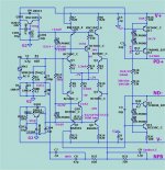
Follow up from early last year. A rough drawn schematic of a power amplifier was posted. That amplifier is now completed and in service with an updated schematic below.
As may have been mentioned earlier, this is a replacement amplifier for a Fisher 600-T receiver. The original circuit was 4 PNP germanium transistors in series to handle the voltage. The circuit was similar to that in an early RCA Transistor Manual and was subject to many problems. Since it used 4 output transistors per channel, it was easy to use parallel devices in the new design.
If I can figure out how to get a picture posted on here, I'll add some info in another post.
Attachments
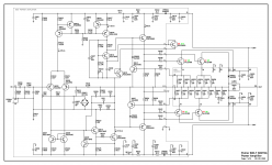
Success in getting the schematic uploaded.
C609-C611 ended up being a slightly unusual arrangement for the Miller capacitor, but it works.
Q613 is clamped to driver Q616 and Q9/Q10 are clamped to Q2/Q6 to control the bias spreader.
Constant current limiting at 4.2 amps is provided by Q614-Q615 and R637-R640. Only one pair of output transistors is sampled, so the total current limit is slightly over 8 amps. The circuit will handle this long enough to blow the 2 amp rail fuses.
R633-R634 connect the driver transistor emitters and the point between them is taken out to a test point. Driver current is 30 mA and eliminates the "speed up" capacitor.
L651 is 11 turns of #22 wire wound around R665.
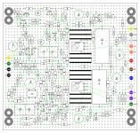
Below is the physical layout. The light green lines are the wires on the back side of the board.
After rereading much of this thread, it appears that VAS transistor, Q611, KSC2690 might be replaced with KSC3503, which has lower Cob.
Since this uses the existing 600-T power supply, rail voltage is ±38 volts, no load. I do not have a distortion analyzer, but output just below visible clipping is 56 watts per channel, both channels driven, 1kHz and below. 10kHz power drops to 52 watts and 20kHz drops to 42 watts.
With a 4 ohm load, power is 66 watts, limited by the 2 amp rail fuses. 2.5 amp fuses might get it up to 100 watts but it would stress the power transformer.
Thanks to Bob Cordell, Douglas Self, Bonsai, and others for all of the valuable information.
C609-C611 ended up being a slightly unusual arrangement for the Miller capacitor, but it works.
Q613 is clamped to driver Q616 and Q9/Q10 are clamped to Q2/Q6 to control the bias spreader.
Constant current limiting at 4.2 amps is provided by Q614-Q615 and R637-R640. Only one pair of output transistors is sampled, so the total current limit is slightly over 8 amps. The circuit will handle this long enough to blow the 2 amp rail fuses.
R633-R634 connect the driver transistor emitters and the point between them is taken out to a test point. Driver current is 30 mA and eliminates the "speed up" capacitor.
L651 is 11 turns of #22 wire wound around R665.
Below is the physical layout. The light green lines are the wires on the back side of the board.
After rereading much of this thread, it appears that VAS transistor, Q611, KSC2690 might be replaced with KSC3503, which has lower Cob.
Since this uses the existing 600-T power supply, rail voltage is ±38 volts, no load. I do not have a distortion analyzer, but output just below visible clipping is 56 watts per channel, both channels driven, 1kHz and below. 10kHz power drops to 52 watts and 20kHz drops to 42 watts.
With a 4 ohm load, power is 66 watts, limited by the 2 amp rail fuses. 2.5 amp fuses might get it up to 100 watts but it would stress the power transformer.
Thanks to Bob Cordell, Douglas Self, Bonsai, and others for all of the valuable information.
Attachments
Lender circuit
In the Audio Amateur article from 1982 Erno Borbely strongly implies that the VAS transistor in the Lender connection is common base. It would seem to be a hybrid as the base is driven as well as the emitter. In Borbely's version the polarity of the followers is changed so the collectors returned to the rails. This makes the voltage across the diff pair collector resistors about the same, for DC analysis.
Has anyone considered whether Borbely's claim has merit?
Jeff
I asked a somewhat related question MANY years ago:
https://www.diyaudio.com/forums/solid-state/2309-power-amp-driver-block-topology.html#post18104
https://www.diyaudio.com/forums/solid-state/2309-power-amp-driver-block-topology.html#post18104
Nelson's post directly below yours is exactly correct. The circuit on the left is not really a cascode in terms of where the dominant action is in controlling VAS current. That circuit is mainly a cute trick to make the collectors of both diff pair transistors see the same VAS input voltage, but it makes very little difference. Both of these circuits are inferior to the IPS/VAS circuit where a current mirror is used.
In a true folded cascode, the limitation is that there is no signal current gain in the VAS. The VAS collector signal current deviation is no greater than the signal current coming from the input pair.
Cheers,
Bob
In a true folded cascode, the limitation is that there is no signal current gain in the VAS. The VAS collector signal current deviation is no greater than the signal current coming from the input pair.
Cheers,
Bob
- Home
- Amplifiers
- Solid State
- Bob Cordell's Power amplifier book