Elso Kwak said:
Hi Evangelos,
But did you compare the sound with my original schematic?
Sorry I did not visit you as I did not travel further than Kalambaka (Meteora)

Hi Elso,
I have not compared the sound, in fact I have not even built the clock - I just breadboarded it to check its operation. I have now designed a PCB and seek for some time to make the board and build the clock. BTW, even in a breadboard form and without using your "trick" 50 ohm probe, the waveform looked perfectly OK in a 30 MHz 'scope.
Your photo reminded me when I was climbing in Meteora - a fantastic place for climbing. I have stopped since 5 years now. I hope that next time you will go more southern
6h5c said:
The 431 circuit uses feedback to regulate the output voltage. The divider is at the output side and provides a feedback to the 431. Any noise produced by the 431 will be present at the output because it's a closed loop, correct me if i'm wrong.
The other circuit has the divider at the input side and doesn't use feedback. The voltage at the base of the BC550 is well filtered by the divider R1/R2 and C3. Nothing more than a passive RC filter. The transistor is a simple voltage follower that provides extra current. My guess is that this transistor produces less noise than a 431 + transistor combination. But of course it may sound worse, i'm hoping to find out
Greetings,
Ray.
Hi Ray,
Sorry for the delayed answer, I' m not that often online.
Regarding the regulator, many "experts" consider the TL431 shunt regulator superior to other series regulators, at least for digital applications. I have used them extensively in my TDA1541 non-oversampling DAC and I' m quite satisfied. I don' t say that I have compared them to other regulators - I neither have the time nor the knowledge to try so many things. I simply follow others' suggestions - people that I estimate them to be a level or two higher than me. So, I just use a previously applied idea or circuit.
Now, my suggestion was that, since the Kwak Clock does not draw large current, one can make the TL431 regulator simpler, that is, without the transistor.
That' s all.
Regards,
Evangelos
Originally posted by kenev
Hi Ray,
Sorry for the delayed answer, I' m not that often online.
Hi Evangelos,
No problem, I was not waiting beside the monitor

Now, my suggestion was that, since the Kwak Clock does not draw large current, one can make the TL431 regulator simpler, that is, without the transistor.
That' s all.
Ah, o.k. Way too much deep thinking on my part. You mean just use it as a pure shunt regulator. Well, it's easy to bypass the NPN on the PCB, when I have it working I'll try it.
I was thinking about a more 'passive' approach.
Maybe i'm going to try more RC or LC filtering (i'm a tubeman...
).Regards,
Ray.
6h5c said:
Ah, o.k. Way too much deep thinking on my part. You mean just use it as a pure shunt regulator. Well, it's easy to bypass the NPN on the PCB, when I have it working I'll try it.
I was thinking about a more 'passive' approach.
Maybe i'm going to try more RC or LC filtering (i'm a tubeman...
Regards,
Ray.
Hi Ray,
I'm a tubeman also, but I never say "no" to SS ideas and implementations. Besides, may "tube gurus" swear on (tubed or SS) shunt regulators. But,, if you try passive filtering without regulation, please let us know your results.
Regards,
Evangelos
kenev said:
Hi Ray,
I'm a tubeman also, but I never say "no" to SS ideas and implementations. Besides, may "tube gurus" swear on (tubed or SS) shunt regulators. But,, if you try passive filtering without regulation, please let us know your results.
Regards,
Evangelos
Hi Evangelos,
I have solid state rectifiers in my amp

And SS current sources

I don't mind mixing things up, as long as the results are good.
And 4x SS diode is so much easier! But I think it will be difficult to get a 5H choke on my clock PCB

Regards,
Ray.
Hi all,
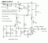
I would like to answer an old forgotten question of Guido. He asked why it is important to supply the Kwak Clock with a symmetric supply.
I think I have an idea. Even, a memory. From the times when I was first playing with this clock. Elso was already at the 6th or 7th version, but me being a lazy guy, first I tried to implement the simple single supply ver. 5, which was reported again by Elso
in this post
While bringing it up, I noticed a discrepancy. The fet oscillator originally would put out a signal with ~5V amplitude, but in the finished clock there appeared only a bit more then 3V. This is due to the loading effect of the comparator input, because we are exceeding it's allowed common mode range [which is 0- 3V for 5V power supply]. This is not a nice thing, and causes a definite distortion in the oscillator signal.
To avoid this is simple: the 1Kohm source resistor should be divided up into two parts, with a 3:2 ratio, or 1:1, if you go for safe.
Then you pick the signal from halfway.
This still not resolves the problem that the osc. signal goes also below ground, as well, though here it's -200mV value is not so bad like the ~1.5V above the common mode limit.
The symmetrical power supplies suggested by Elso, and the additional DC shifting of the signal does resolve completely this problem, so I can imagine that the problem pointed out above was / is the cause for the experienced better sound.
For the lazy types the above correction might be still useful.
Ciao, George
Hi George, I never measured that high amplitudes of signal at the FET.
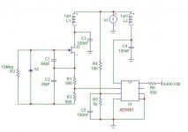
I discovered that a dual supply for the AD8561 in a SPDIF receiver gave better sound. Here the amplitude is 0.5V peak-peak. Then I applied this to my clock. If you occasionally have too high output from the FET you can lower the source resistor but if you go too low you run into starting up problems. With a higher frequency fundamental crystal the amplitude is quite low, with say 11.2896MHz it is pretty high. I tried to obtain values that satisfy all CD-frequencies.
I discovered that a dual supply for the AD8561 in a SPDIF receiver gave better sound. Here the amplitude is 0.5V peak-peak. Then I applied this to my clock. If you occasionally have too high output from the FET you can lower the source resistor but if you go too low you run into starting up problems. With a higher frequency fundamental crystal the amplitude is quite low, with say 11.2896MHz it is pretty high. I tried to obtain values that satisfy all CD-frequencies.
Elso,
I have just measured >5V, with 5V power supply. Also the sims gave that. I did not want to post without controlling. Did you measure the signal with the jfet source disconnected from the comparator inp? [pin2] Try it please. And then reconnect.
Because one pic is better than a page of explanations, I've made a short demo drawing of what I'm talking about.
But anyway, this is only a mod for the lazy, like 6h5c..
Otherways your standard version works. I only brought this up, because it may be an explanation.
Ciao, George
Joseph K said:Hi all,
While bringing it up, I noticed a discrepancy. The fet oscillator originally would put out a signal with ~5V amplitude, but in the finished clock there appeared only a bit more then 3V. This is due to the loading effect of the comparator input, because we are exceeding it's allowed common mode range [which is 0- 3V for 5V power supply]. This is not a nice thing, and causes a definite distortion in the oscillator signal.
For the lazy types the above correction might be still useful.
Ciao, George
Hi George,
Just to disprove my lazyness, I switched on my scope at 7:15 AM, after I read your posts
I measured an amplitude of 4,5Vpp with and without the comparator present, so I don't see the loading effect here. How could that be possible anyway, since the inputs are high impedance?
The frequency is 16,9...MHz. Are you also using a J310?
You measure an output amplitude >5V with only single 5V supply, how is that possible? Could this be an inductive problem, like the boost in voltage you get in a resonance circuit (the term in dutch is "opslingering", but I don't know in english
). Also you speak of the signal going below ground, how is that possible, since there's no coupling cap?Questions, questions, questions.......but then again, I don't have a degree in HF electronics....
Greetings,
Ray.
Dear 6h5c,
I hope You did understand that I was joking? The greatest lazy one is me myself..
But, and DOH! I drew a blank here, again! When I was reporting of the measurements, I did not finish only the oscillator [in a new setup, the old one is working at home], so I was sure about the osc. level, but was going by memory on the interfacing problem.. Which, I feel constrained to repeat, I had definitely experienced in the past.. But not now. 6h5c is right, there is only a small difference in the oscillation levels between comparator connected // not connected. And there is no visible distortion / load effect on the signal. In the past days I lost some time trying to recreate my past experience, but was not succesfull.
Though my claims are more or less supported by the data sheets. Now I did a bit more digging into this, and seems that when the guaranteed common mode levels are exceeded, two things could happen: the input impedance changes, and the internal timing changes. The first one should be seen on the signal waveform, the second one..? jitter parameters changing?
Here I understood that specially in case of the AD8561, which is pnp input config, the positive going signals does not suffer / suffer less from changing impedance, because it is growing. Instead, the negative going half should be more sensitive to this problem.
Now, I don't know. If you decrease the input swing according to my scheme, you get safer in this reference, in any way. But, get worse 6db signal/noise ratio, which is an important factor, as well..
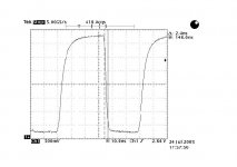
What regards the exact levels, 6h5c, I think here there is a lot of uncertainty in depending on the particular realization / measurement tools. So as to counter somehow my previous stupidity, I would enclose here some graphs.. some of which might be interesting.
So, first the oscillator output in the Kwak Clock, measured on pin 2 of the [connected] comparator. The power supply, measured with the same scope probe, is 5.02 V. Notice the base shift of the signal versus negative.
I hope You did understand that I was joking? The greatest lazy one is me myself..
But, and DOH! I drew a blank here, again! When I was reporting of the measurements, I did not finish only the oscillator [in a new setup, the old one is working at home], so I was sure about the osc. level, but was going by memory on the interfacing problem.. Which, I feel constrained to repeat, I had definitely experienced in the past.. But not now. 6h5c is right, there is only a small difference in the oscillation levels between comparator connected // not connected. And there is no visible distortion / load effect on the signal. In the past days I lost some time trying to recreate my past experience, but was not succesfull.
Though my claims are more or less supported by the data sheets. Now I did a bit more digging into this, and seems that when the guaranteed common mode levels are exceeded, two things could happen: the input impedance changes, and the internal timing changes. The first one should be seen on the signal waveform, the second one..? jitter parameters changing?
Here I understood that specially in case of the AD8561, which is pnp input config, the positive going signals does not suffer / suffer less from changing impedance, because it is growing. Instead, the negative going half should be more sensitive to this problem.
Now, I don't know. If you decrease the input swing according to my scheme, you get safer in this reference, in any way. But, get worse 6db signal/noise ratio, which is an important factor, as well..
What regards the exact levels, 6h5c, I think here there is a lot of uncertainty in depending on the particular realization / measurement tools. So as to counter somehow my previous stupidity, I would enclose here some graphs.. some of which might be interesting.
So, first the oscillator output in the Kwak Clock, measured on pin 2 of the [connected] comparator. The power supply, measured with the same scope probe, is 5.02 V. Notice the base shift of the signal versus negative.
Attachments
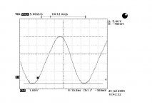
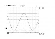
Nice, eh? Now I can admit, that it was a pain to get it.. That is, to arrive to this, one should have the right instrumentation. Here I would enclose the same thing, but with the standard [though still better than average scope probe]
I hope it is more familiar..
I hope it is more familiar..
Attachments
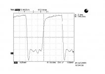
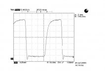
Now I can disclose the difference: the first graph was taken by a Tek P6243 fast/active/divide by ten probe, having, most importantly, < 1pF input capacitance, 1Meg input impedance, 1G bandwith - and a local springy ground lead applied.
The second, standard case was taken by a Tek P6137, Only 400 Mhz, but most importantly, 10.8 pF/ 10Meg input impedance, with the usual, or still better than usual ~10cm ground lead. Which I tried to wrap up / fit tight, but it's impossible.
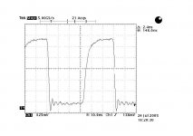
So as to see which is the bigger problem, the ground lead or the input capacitance, I tried to place a small variable cap on the Qout. with this having a ~4pf [minimal ] value, the situation is the following:
The second, standard case was taken by a Tek P6137, Only 400 Mhz, but most importantly, 10.8 pF/ 10Meg input impedance, with the usual, or still better than usual ~10cm ground lead. Which I tried to wrap up / fit tight, but it's impossible.
So as to see which is the bigger problem, the ground lead or the input capacitance, I tried to place a small variable cap on the Qout. with this having a ~4pf [minimal ] value, the situation is the following:
Attachments
- Status
- This old topic is closed. If you want to reopen this topic, contact a moderator using the "Report Post" button.
- Home
- Source & Line
- Digital Line Level
- Can someone send to me the Elso's latest clock schematics (version6)? :)