PNP transistor, emitter still connected to ground? Sorry for all the seemingly simple questions...just want to be sure. I hate to see stuff smoke. I was thinking of using a gyrator in the PS prior to the reg, but I've never seen one for negative voltage? Would it be worth doing? I don't have chokes to use, I'm using a CRC filter.
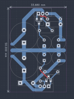
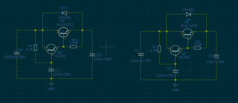
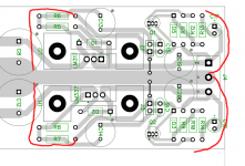
I've put together a PCB for a dual rail, centre-tapped transformer version for my own use. It's single sided as I enjoy etching board myself.
I would be grateful if anyone might cast an eye over the layout and double chec my work before I make a test board up.
Many thanks.")
I would be grateful if anyone might cast an eye over the layout and double chec my work before I make a test board up.
Many thanks.
Attachments
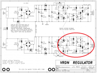
Have a look at Mark's VRDN project:PNP transistor, emitter still connected to ground? Sorry for all the seemingly simple questions...just want to be sure. I hate to see stuff smoke. I was thinking of using a gyrator in the PS prior to the reg, but I've never seen one for negative voltage? Would it be worth doing? I don't have chokes to use, I'm using a CRC filter.
Anything can be reversed, including a gyrator: simply reverse the polarity of everything. You can keep the same PCB if the pinouts are the same.
Cannot work with tube circuits obviously
Something wrong there: the emitters of the correction transistors go to Vout instead of GNDI've put together a PCB for a dual rail, centre-tapped transformer version for my own use. It's single sided as I enjoy etching board myself.
I would be grateful if anyone might cast an eye over the layout and double chec my work before I make a test board up.
Many thanks.
A gyrator will give you ~60dB additional PSRR, compared to ~30dB for the denoiser.I was thinking of using a gyrator in the PS prior to the reg,
Thus, a gyrator would appear to be 30dB better, but there are other aspects to consider: a gyrator will only act on ripple, but the denoiser also improves all the rest by 30dB: output impedance, but more importantly the wideband noise.
In fact, with a gyrator the hum will be completely buried below the noise level, but the overall output crap will be larger compared to a denoiser.
A gyrator will also need an additional ~2V dropout voltage to work properly. The denoiser will work exactly like an unmodified regulator regarding the DC conditions.
I've put together a PCB for a dual rail, centre-tapped transformer version for my own use. It's single sided as I enjoy etching board myself.
I would be grateful if anyone might cast an eye over the layout and double chec my work before I make a test board up.
Many thanks.
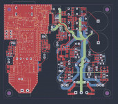
I see V+ and V- go on the outside. It would be better to route them close to the GND trace on each side of it. This way you have the denoiser out of the current loop.
R6/R7 don't need the ground on the output connector, you can ground them right next to them.
J2/J3 the same, they ground the 220uF cap for Cadj config. You're better off grounding those closer to the input caps. Also rotate C13/C14 so pins are aligned vertically and put J2 between R6/C13, same on the negative side.
If you route the outputs next to the ground trace, you'll also have to reconfigure the whole denoiser circuit layout, output caps will also have to be behind the connector somewhere. The idea is to keep the denoiser circuit out of the V+-/GND loops.
edit: also make sure the CAD software has the correct pinout for the small BJT. Double check the pinout of the transistors you are actually going to use (eg BC3x7).
also maybe you could consider a simple capacitance multiplier instead of the large CRC pack. the board could be shorter this way.
Last edited:
Something wrong there: the emitters of the correction transistors go to Vout instead of GND
I see V+ and V- go on the outside. It would be better to route them close to the GND trace on each side of it. This way you have the denoiser out of the current loop.
R6/R7 don't need the ground on the output connector, you can ground them right next to them.
J2/J3 the same, they ground the 220uF cap for Cadj config. You're better off grounding those closer to the input caps. Also rotate C13/C14 so pins are aligned vertically and put J2 between R6/C13, same on the negative side.
If you route the outputs next to the ground trace, you'll also have to reconfigure the whole denoiser circuit layout, output caps will also have to be behind the connector somewhere. The idea is to keep the denoiser circuit out of the V+-/GND loops.
edit: also make sure the CAD software has the correct pinout for the small BJT. Double check the pinout of the transistors you are actually going to use (eg BC3x7).
also maybe you could consider a simple capacitance multiplier instead of the large CRC pack. the board could be shorter this way.
Thank you chaps, I'm grateful for your time.
It seems a bit of major redesign is in order then, this is just the sort of help I was after.
I quickly drafted an example for a dual capacitance multiplier.
For a 50mm width for your board, it would need roughly 34mm in length, instead of the whole CRC arrangement you already have in your design.
it keeps the same logic for the pcb design with GND in the middle.
I have included a spice sim so you can compare with a CRC design. For the same Vdrop of around 1.7V you have better PSRR at 100-120Hz. Sim is for around 600mA. Higher/lower current will affect Vout of CRC.
The board design is an example on how it would look on the board.
edit: also you need to consider you output current. for lower currents there's no need for a heatsink. Considering 1.5Vdrop across the pass transistor you can figure out how much heat it dissipates at your required output current, and add a heatsink or not.
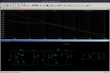
if you need lower Vdrop (~1.2V) across cap multi you can consider a Sziklai pair arrangement for the capacitance multiplier (second sim photo).
For a 50mm width for your board, it would need roughly 34mm in length, instead of the whole CRC arrangement you already have in your design.
it keeps the same logic for the pcb design with GND in the middle.
I have included a spice sim so you can compare with a CRC design. For the same Vdrop of around 1.7V you have better PSRR at 100-120Hz. Sim is for around 600mA. Higher/lower current will affect Vout of CRC.
The board design is an example on how it would look on the board.
edit: also you need to consider you output current. for lower currents there's no need for a heatsink. Considering 1.5Vdrop across the pass transistor you can figure out how much heat it dissipates at your required output current, and add a heatsink or not.
if you need lower Vdrop (~1.2V) across cap multi you can consider a Sziklai pair arrangement for the capacitance multiplier (second sim photo).
Attachments
-
 Screenshot_20211031_175207.png92.4 KB · Views: 555
 -
 Screenshot_20211031_175235.png181.1 KB · Views: 536
 -
 Screenshot_20211031_180812.png77.1 KB · Views: 539
 -
 Screenshot_20211031_182303.png87.9 KB · Views: 528
 -
cap_multi vs crc.asc4.1 KB · Views: 71
-
 Screenshot_20211031_182912.png37.6 KB · Views: 534
Last edited:
If you want to add a cap-mult to a denoised regulator, you have to place it before the regulator, otherwise you will lose the denoiser's benefits: low impedance and low noise.
Without a denoiser, you have to chose your evil: upstream you will keep the relatively good impedance of the regulator, but you will also get its unabated noise, downstream you will degrade the impedance but improve the noise (without arriving at the denoiser's performance though).
Trileru has shown some examples of cap-mult + denoiser in this thread.
Performances are stellar, but it comes at a cost: you waste ~4V dropout voltage (plus the complexity).
A dienoiser arrives at the same level practically (a 180dB PSRR is ~meaningless) but without the drawbacks
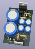
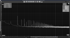
Made a new version for my DAC, still using the CS4398. This time I completely removed the SPDIF transport. I'm using a HDMI cable between DAC and Raspberry Pi shield (that I also made). I have a 24.576MHz oscillator and a 8 bit synchronous counter which I set for 96KHz output from DAC (fixed). LVDS drivers move BCLK/LRCK from master clock to Raspberry Pi and the audio data from Pi to DAC. The shield has ADUM210N isolators for all three lines. Pi is slave and signal gets reclocked on the DAC board before getting into the DAC chip itself.
Seems to work fine so far. I measured all rails and they seem to work fine.
LM317 + dienoiser is usable for 5V VACC.
The opamp supplies are the discrete regulator version, with ccs dienoiser.
I attached the measurement for 5V LM317+dienoiser rail.
Also this time I removed the power transformer from the case, but was still next to the board while measuring with no case.
Attachments
I quickly drafted an example for a dual capacitance multiplier.
Thank you Trileru, very kind of you to take the time.
Trileru has shown some examples of cap-mult + denoiser in this thread.
Performances are stellar, but it comes at a cost: you waste ~4V dropout voltage (plus the complexity).
A dienoiser arrives at the same level practically (a 180dB PSRR is ~meaningless) but without the drawbacks
Thanks Elvee, the thinking behind the CRC filter wasn't so so much from a ripple rejection point of view but rather reducing the amount of high frequency noise coming in from the rectifiers. I may well be wrong on this but I understand that filtering the saw tooth like ripple with a CRC to a more sinusoidal ripple filters out the higher frequency mains harmonics, which regulators and op amps find harder to filter out than mains frequency ripple?
In any event I've attached a new PCB layout based on Trileru's layout advice in post #2290. The positive and negative rail traces now run parallel to the ground trace and the denoiser circuitry is outside the current loop.
Should C15 and C16 ideally ground after the output capacitors C19 and C20 and not before, as in the current design, like a sort of Kelvin connection arrangement?
Attachments
You could rotate R6/R7 and ground them next to C8/C12, so as to not carry that trace to the output. Maybe even swap positions between R5/R6 and R7/R8.
Also you'd want to put the sensing point as close to the output connector as possible. V+/V- you're sensing right on the output, but you're sensing the ground a bit back.
Also you should consider the V+/GND and V-/GND sense lines loops as well. To keep them close together you could take the GND from the output connector as I show in the attached photo. You'd have to play a bit and see if it isn't hard to route it that way. Also ideally the sense lines would be kept short. V+/V- are ok, maybe the GND sense lines don't come out too long the way I show in the photo. Else seems ok to me. At this point you're gilding the lily anyway.
edit: R11/R9 are not sense, they provide the current for the denoiser. Sensing is through C17/C18, that should be from the output connector (as it is now). R11/R9 can be connected on the output cap V+/V-. Also rotate C17/C18 (says my OCD).
2nd edit: if you're worried about HF then maybe use a CLC instead of CRC. I still think you don't need that much capacitance on the input. Pretty sure you can safely drop half of the capacitors. How much current will the supply provide at max? Also make sure the positive output cap has an ESR of around 0.2ohms and the negative output one lower than that (maybe 0.1ohms).
Attachments
Last edited:
- Home
- Amplifiers
- Power Supplies
- D-Noizator: a magic active noise canceller to retrofit & upgrade any 317-based V.Reg.