Awesome work, Jean-Marc and Christophe - watching your efforts
with great interest. Appreciate the board being released under CC-BY-SA 4.0 license.
Looking forward to the final result")
Thanks for your support Quadtech. Happy to see interest in this project.
Lot of progress today, will update tomorrow.
Chris
Hi,
I just took a quick look on the pictures of your PCBs and the layout recommendations in the tas3251 datasheet.
On the first view that reference design doesn't really look that well thought out. I think the routing could be improved. Especially because the chip doesn't have a power pad on the bottom side.
Those vias routing the amp outputs to bottom in the datasheet are rather of a symbolic value. I think that should symbolise that there will be vias needed. Those 5 vias will not really be capable of handling 175 W per channel. I think you should use much more vias or filled ones or what would be the best, route the power lines on top without vias to bottom.
Sure that the design can be improved. This is the the expected benefit from open harware. However, it looks like if it is implemented like this in the TI EVM board, which is the reference for the output part of the design. For me, it is incredible how so much power can be drawn from such a small footprint. And when yo see the size of the chip pins... I wonder about the output power.
So, after solving a "bad" solder on the /FAULT pin, it seems that at least the TAS3251 is alive. I can set the DSP registers with the I2C. However I still keep the power part down.
Tomorrow, I will try to activate the power part (/ Reset_Amp high).
I paid attention to Christophe finding that the default I2S word length is 24 bits and not 16 like my USB to I2S board. This parameter does not looks configured through PPC3, which is surprising for me, as it is an important parameter. Well found Christophe !
Have also to work on the heatsink, to be more comfortable with the thermal aspect.
JMF
Today update :
Volume potentiometer removed and replaced by a rotary encoder.
Balanced the overall gain chain, volume is now controled by the DSP reg0x44 & 0x48.
Fixed some bugs.
Added erase command.
Produced documentation here attached
Remaining :
Implement a logarithmic law on volume control
Handle TAS Fault and ClipOn error
Then, it'll be time to start using the software to start playing with the DSP.
Volume potentiometer removed and replaced by a rotary encoder.
Reading was too unstable for low values (when center tap was close to the zer), and noise suppression algorithm was introducing a too large dead angle.
Added a multicolor status led and the pushbutton of the encoder to have a basic UI. Pushbutton allows to store current volume in memory.
Balanced the overall gain chain, volume is now controled by the DSP reg0x44 & 0x48.
Fixed some bugs.
Added erase command.
Produced documentation here attached
Remaining :
Implement a logarithmic law on volume control
Handle TAS Fault and ClipOn error
Then, it'll be time to start using the software to start playing with the DSP.
Attachments
On EVM Board, the XMOS and the MSP430 uC are both connected to the I2C bus of the TAS3251. Your plan make the assumption that the MSP430 is not involved in TAS setup, but this is very unlikely. Even if it's the case you'll have to know the protocol used between PPC3 and the sofware within the XMOS : you'll need the TI XMOS software of the EVM...
On EVM Board, the XMOS and the MSP430 uC are both connected to the I2C bus of the TAS3251. Your plan make the assumption that the MSP430 is not involved in TAS setup, but this is very unlikely. Even if it's the case you'll have to know the protocol used between PPC3 and the sofware within the XMOS : you'll need the TI XMOS software of the EVM...
I have bought an EVM board, is there a way to disable MSP430, only left XMOS and TAS3251 to verify this function?
I only see how to disable XMOS function in manual.
thanks.
I have bought an EVM board, is there a way to disable MSP430, only left XMOS and TAS3251 to verify this function?
I only see how to disable XMOS function in manual.
thanks.
My understanding is that there is a jumper for a "slave mode", and that this jumper should disable at least part of the MSP430. However this is not so well documented and I don't have such a board.
JMF
I just took a quick look on the pictures of your PCBs and the layout recommendations in the tas3251 datasheet. On the first view that reference design doesn't really look that well thought out. I think the routing could be improved. Especially because the chip doesn't have a power pad on the bottom side.
For me, it is incredible how so much power can be drawn from such a small footprint. And when yo see the size of the chip pins... I wonder about the output power.
Wonder why TI doesn't double up the high current pins (PVDD/SPK_OUT) to address cooling and routing issues? Like GND - same signal multiple pins. Perhaps they prioritize small package / fewer pins.
Is there a reason why most designs go for 15V first, and then 12 and 3.3V? Is it noise?
On EVM, the 15V produced by the LM5010 is not very clean, I get up to 100mV of ripple (our board is a copy of EVM supply section) . It's may be required to have a clean 12V for gate drive produced by a linear regulator. As amp supply may goes to 36V, a 12V linear will have to dissipate a lot of power, so a switching pre regulator may be relevant.
Would be interesting to try a 12V switching supply for (G)VDD, in place of the LM5010 15V switching and LM2940 12V linear stages. May not produce the cleanest power, but will consume less.My explanation of the 15V step is that it is done like that in the TI EVM board. Doctormord had in mind it could be skipped. But I didn't dared to do it. However it is not an expensive part.
Also interesting is the TI PMP30183 PSU reference design with 30/12/3.3VDC outputs.
[...] TAS play very loud and there’re many (at least 3) volume control stage in the signal path. The analog one (0/-6dB selector) and the basic digital one (Reg0x3D-3E, B0/P0) are documented but not the one to use (Reg0x44-0x48, Page x01e) within the biquads area. Question : which balance for the best dynamique and SNR ?. For now I have -6dB analogic, -44dB digital, +24dB default TAS gain and my volume control based on Reg0x44 and 0x48 biquads.
Do you not find the basic digital volume control ("DAC Digital Gain Control" registers 0x3D/0x3E) to be adequate? It seems useful for most applications. It appears isolated to the DAC stage, post-DSP (and separate from the DSP volume block, registers 0x44/0x48). As for analog gain (register 0x02), is it wrong to speculate that -6 dB may reduce dynamic range (default is 0 dB)? Also part of the analog stage is 10% gain "amplitude boost" (register 0x07). In any case, your work is very helpful.Balanced the overall gain chain, volume is now controled by the DSP reg0x44 & 0x48.
Last edited:
another question:
if I only input I2S signal from Bluetooth to TAS3251 but the RESET_AMP, DAC_MUTE, CLIP_OTW, FAULT and I2C signals are floating, would TAS3251 works properly?
Or I still need MCU to write data through I2C to start up the TAS3251 anyway.
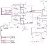
The attachment is part of the schematic.
if I only input I2S signal from Bluetooth to TAS3251 but the RESET_AMP, DAC_MUTE, CLIP_OTW, FAULT and I2C signals are floating, would TAS3251 works properly?
Or I still need MCU to write data through I2C to start up the TAS3251 anyway.
The attachment is part of the schematic.
Attachments
another question:
if I only input I2S signal from Bluetooth to TAS3251 but the RESET_AMP, DAC_MUTE, CLIP_OTW, FAULT and I2C signals are floating, would TAS3251 works properly?
Or I still need MCU to write data through I2C to start up the TAS3251 anyway.
The attachment is part of the schematic.
You absolutly need to manage most of those lines to cope with:
- configuration of the DSP (default won't produce sound),
- powering sequence (especially RESET_AMP)
- fault management is I believe necessary for robust operation.
The TAS5825 can load configuration from an EEPROM and may be less in need of a uC.
For me TAS3251 definitly needs to be controlled by a processor (on board or off board).
JMF
Yes
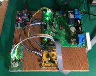
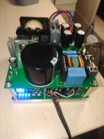
Second board working and making sound.
After some software trials and errors for the I2C configuration of the TAS3251, the board makes sound, with a basic configuration. It is configured using Arduino IDE (quite easy).
AIM65 has been very helpull by providing a proven config file (registers/values) and some measurements of interest for troubleshooting.
I will track them here (credit to AIM65 for most of them):
- Registers of interest for troubleshooting are: 0x02, 58, 5b, 5c, 5d, 5e, 5f
- if voltage at CPVSS (C19) is not -3.3V, then there is a problem in the clock configuration,
- most of the troubleshooting can be done with RESET_AMP low (so with the power section down),
- check that the I2S source is providing the clocks. No I2S clocks <=> DSP down and not possible to configure it,
- don't forget to action DAC_MUTE in the power sequence, event if it is not listed in datasheet section 8.3.11.1 Power Up and Startup Sequence.
Measured onsumptions (power supply 18V, low volume, values are the displays of the low cost lab power supply):
- /RESET_AMP low, DSP not operational: about 60 mA
- /RESET_AMP low, DSP operational: about 0.9 mA (to be rechecked)
- /RESET_AMP high, amp working : 190mA
Some timings look a bit sensitive. May need exploration.
I will upload pieces of code in coming days on Home * jmf13/NeatAmpTAS3251 Wiki * GitHub
JMF
Last edited:
Would be interesting to try a 12V switching supply for (G)VDD, in place of the LM5010 15V switching and LM2940 12V linear stages. May not produce the cleanest power, but will consume less.
Also interesting is the TI PMP30183 PSU reference design with 30/12/3.3VDC outputs.
Yes, agreed, this 15-12V intermediary step down could certainly be removed.
The PMP30183 ref design looks like a good companion of TAS3251, with a close to 4 peak factor.
Do you not find the basic digital volume control ("DAC Digital Gain Control" registers 0x3D/0x3E) to be adequate? It seems useful for most applications. It appears isolated to the DAC stage, post-DSP (and separate from the DSP volume block, registers 0x44/0x48). As for analog gain (register 0x02), is it wrong to speculate that -6 dB may reduce dynamic range (default is 0 dB)? Also part of the analog stage is 10% gain "amplitude boost" (register 0x07). In any case, your work is very helpful.
Thank you for asking, answering your question allows me to reconsider the way I implemented volume.
If we consider all the filters and DSP effects in the TAS DSP set to 0dB (except volume control), gain chain is :
DSP volume control (Book0x08c-Reg 0x44-7/0x48-b) [-LdB -> + HdB] + DAC digital gain (Book0x0-Reg 0x3d/0x3e) [-110dB –> +24dB] + Analog gain [-6dB/0dB] + Analog boost [0dB/+0.8dB]
L and H are unknowns, basic tests have made shows that L and M are large enough to provide effective volume control.
According to datasheet, DAC digital gain provide a linear relationship between gain in dB and register value.
The DSP Volume control provide a linear relationship between transfer ratio and register value thus a logarithmic relationship between gain in dB and register value. To get that linear relationship that a volume potentiometer should implement, I had to add math.h library nd pow function to my software which immediately grab me 5 kbytes of flash memory…
Without any specific clue to choose DAC gain or DSP volume, I’ll switch back volume control to the DAC digital gain registers and set the DSP ones to 0dB.
The TAS5825 can load configuration from an EEPROM and may be less in need of a uC.
The TAS5825M can indeed load part of its configuration from an SPI EEPROM, but this is not the case of the book 0. In addition to that the load from the EEPROM has to be initiated through I2C. This feature only allows loading configuration faster and a MCU is still needed to get it working, it can't work autonomously.
Excellent work on the startup ballet.
Perhaps a floating DAC_MUTE pin is forced low via internal pull-down resistor for safety. The datasheet refers to XSMT (soft mute pin on other TI chips) instead of DAC_MUTE in some places. DAC_MUTE/XSMT/register 0x03 are likely tied together internally.
Been searching for a suitable 36V primary / 12V aux SMPS. The PMP30183 design is not produced commercially. Looking at Connex Electronic SMPS800RS, Queenway G-005 / G-015 (Aliexpress), and Daitron low noise LFS series (30V no aux).
In case you revisit DSP volume control... May want to check compiler flags to optimize for size if it includes too much from math.h. A loop-based pow() function can be implemented if that's all you need. Sometimes it's best to use a lookup table (array) instead of recomputing for every sample.
Excellent work on the startup ballet.
Perhaps a floating DAC_MUTE pin is forced low via internal pull-down resistor for safety. The datasheet refers to XSMT (soft mute pin on other TI chips) instead of DAC_MUTE in some places. DAC_MUTE/XSMT/register 0x03 are likely tied together internally.
Been searching for a suitable 36V primary / 12V aux SMPS. The PMP30183 design is not produced commercially. Looking at Connex Electronic SMPS800RS, Queenway G-005 / G-015 (Aliexpress), and Daitron low noise LFS series (30V no aux).
In case you revisit DSP volume control... May want to check compiler flags to optimize for size if it includes too much from math.h. A loop-based pow() function can be implemented if that's all you need. Sometimes it's best to use a lookup table (array) instead of recomputing for every sample.
Yes,... I'v seen XSMT written here and there in this totally nuts datasheet full of cust/paste coming from other TI chips. Having the TAS plyaing sound is kind of an escape game with this paper !, unless you already knows other TI products from their Class D portfolio.
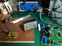
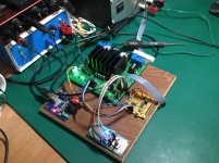
Aluminium
After <math.h>, I switched to some metalwork today.
As often the tool, the screw tap broke on the last hole, so I've only 3 on 4 screw to link the pad and the heatsink...it'll be alright.
Tests with 27V switching PSU and real speakers are planned for tomorrow.
After <math.h>, I switched to some metalwork today.
As often the tool, the screw tap broke on the last hole
, so I've only 3 on 4 screw to link the pad and the heatsink...it'll be alright.Tests with 27V switching PSU and real speakers are planned for tomorrow.
Attachments
...
Been searching for a suitable 36V primary / 12V aux SMPS. The PMP30183 design is not produced commercially. Looking at Connex Electronic SMPS800RS, Queenway G-005 / G-015 (Aliexpress), and Daitron low noise LFS series (30V no aux).
....
I'm not really proficient about power supplies. As of today, my intention is to purchase a MEAN WELL LRS-350-36. Suitable and excellent quality/price ratio (44€).
But this looks suboptimal compared to a "designed for" power supply like the PMP30183 design: sized for average power, but fit for peak power.
However this seems difficult to build because of specific transformers and coils. They seem to be produced by Würth but they didn't answered to my query email last time I looked at that.
Would be so nice to have an open DIY design for such a switching power supply...
JMF
Would be so nice to have an open DIY design for such a switching power supply...
JMF
??? ??????? ????????? ? ??????????? TPA3255 c ???
I do LLC PSU for TPA3251 amp
Attachments
Last edited:
- Home
- Amplifiers
- Class D
- [design log] Neat 2x170W I2S in, I2C controlled, integrated DSP amp (TAS3251)