54kHz and 16kHz as pole?Stellema solved it with two-pole compensation (at 16KHz and 54KHz). That is impressive.
Off the top of my head I can't confirm this, is there nothing more than a more or less additional capacitive load on the IP and VA? , of course the phases rotate ...
Help,
I may have put on the wrong glasses.

THX
The poles are easy to compute due to the resistor loading.
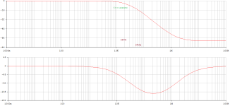
The 16KHz pole is formed by C8, R13, R7, R16, and R17.
The 53KHz pole is formed by C13, R26, R3, and R4.
For readers of this thread, the "TIM doctrine" should be interpreted as "Keeping the poles above 20KHz guarantees that the open-loop gain will be sufficient (if the DC gain is sufficient) and the amplifier cannot slew on audio signals."
Ed
Last edited:
Many thanks Ed,
I sat down in front of the Stellema circuit diagram again with "paper and pencil" (just for fun and as a little exercise).
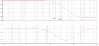
Poles 18.6637kHz & 56.139kHz; the differences are probably due to the fact that I tried again to form a middle transistor (from classes A,B and C) and carried out a source observation. So I also consider the internal resistances, input and output side and transform the local negative feedback of the strange, last VA ...
In the text we read that the OL bandwidth was set at 15kHz.
Honestly (and this is not an attack either), I have problems with the term frequency response compensation in this case, for me the chosen method is nothing more than a complex load.
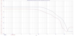
Its effect alone looks like in the file attachment, I chose the amplitude and phase response (frequency response) as a means of description because it is so nicely illustrative. In the open loop case, of course, without the influence of all other parameters.
Regards,
HBt.
I sat down in front of the Stellema circuit diagram again with "paper and pencil" (just for fun and as a little exercise).
Poles 18.6637kHz & 56.139kHz; the differences are probably due to the fact that I tried again to form a middle transistor (from classes A,B and C) and carried out a source observation. So I also consider the internal resistances, input and output side and transform the local negative feedback of the strange, last VA ...
In the text we read that the OL bandwidth was set at 15kHz.
Honestly (and this is not an attack either), I have problems with the term frequency response compensation in this case, for me the chosen method is nothing more than a complex load.
Its effect alone looks like in the file attachment, I chose the amplitude and phase response (frequency response) as a means of description because it is so nicely illustrative. In the open loop case, of course, without the influence of all other parameters.
Regards,
HBt.
Attachments
@wahab
Would you like to share the transistor models you used in post #32 with the rest of us? And share here as *.txt file. That would be wonderful, then we would have a common denominator in the analysis of the Stellema construct.
By the way, how do you like my quick, alternative IP-VAS #229 idea?
Would you like to share the transistor models you used in post #32 with the rest of us? And share here as *.txt file. That would be wonderful, then we would have a common denominator in the analysis of the Stellema construct.
By the way, how do you like my quick, alternative IP-VAS #229 idea?
Last edited:
One final (unintentionally) confusing addition to the pole view alone.
Last night I calculated the resulting 19.783kHz from my poles for the theoretically expected -3dB corner frequency of the negative feedback path. Ed's clues resulted in 16.752kHz.
I must have made a mistake in the absolutely theoretical consideration and the formulation of the solution equation ... or the perspective taken is inadmissible!
But the simulation seems to prove me right, even if the result is of course not the real Stellema.
Attachments
@wahab
Would you like to share the transistor models you used in post #32 with the rest of us? And share here as *.txt file. That would be wonderful, then we would have a common denominator in the analysis of the Stellema construct.
By the way, how do you like my quick, alternative IP-VAS #229 idea?
Basically you re on the road of the usual differential + common emitter VAS albeit enhance in this case,
i m waiting for some real simulation to see, or rather confirm, the characteristics of this ubiquitous
circuit back in the 70s.
In the waiting here are the spice model from Phillips, the first one is from phillips themselves
while the second one seems to be just a copy that is used in the Simetrix simulator library.
Attachments
I will definitely not keep the strange IP-VA-stage.(...) the characteristics of this ubiquitous circuit back in the 70s.
I don't even want to know exactly what the Australian... At most, I invest time in the quick shot from posting #229 and the diamond power amp.
No matter how far you /we dive into the depths of the optimization abyss (in the simulator), the original circuit cannot be put on the right path of virtue.
There is also no potential for morphing. You can take the output stage and practically feel its teeth ("auf den Zahn fühlen") and nothing more.
Possibly some kind of Krill (see Steve Dunlap) is successful, as I have already said.
In any case, a good design looks very different. In my enthusiasm for the bizarre, I fell for the article.
Sorry,
HBt.
a quick thought - in the rush of depth

Apparently I don't want to leave L.Stellema to the abyss and want to save the HP amp - the team starts the last attempt.
@wahab,
what do you think about this rescue plan, it could be promising.
If the deep intoxication has already taken over, I go into the pressure chamber and take a cure.
HBt.
Apparently I don't want to leave L.Stellema to the abyss and want to save the HP amp - the team starts the last attempt.
@wahab,
what do you think about this rescue plan, it could be promising.
If the deep intoxication has already taken over, I go into the pressure chamber and take a cure.
HBt.
And it does work - here is the first deep-sea submarine (from the planning office)!
Features
extremely broadband,
follows the original as far as possible without the inherent level shifter function
strict separation of IP, VA, OP stage
no parasitic oscillation

Features
extremely broadband,
follows the original as far as possible without the inherent level shifter function
strict separation of IP, VA, OP stage
no parasitic oscillation
Attachments
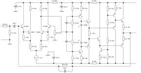
I still see the resistor voltage divider biasing and ac coupling for the "vas"without the inherent level shifter function
I understand your objection Bernard, the present construction looks damn similar to the original (which is what I intend, of course not at any price - basically I don't like this shape any more than you do), but the junction point is exactly at half the operating voltage, i.e. zero volts.I still see the resistor voltage divider biasing and ac coupling for the "vas"
On both coupling sides, the IP and the VA, in the separate state of the stages. The DC-loop now only minimally corrects the entire offset, as we are already at zero.
Last edited:
If the present case were a real, pure AC coupling, as one would imagine a coupling capacitor to be, then 1µ would be much too small. And with the (low-impedance) dynamic load of the IP, a coupling capacitor would have to be 1mF in size.
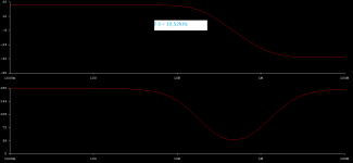
The bode plot looks exemplary in any case, even without the 1µ capacitors.
The bode plot looks exemplary in any case, even without the 1µ capacitors.
Thank you for this hint Bernard.My only intention here is to see about what THD could be expected.
No care has been taken for things like clipping behaviour, thermal stability...
I myself, am always interested in the THD (or TIM) very late in a design study, the static case, i.e. at idle, comes first for me, followed by the steady state, then the dynamic range.
Then the time response, i.e. how the system reacts to different excitation functions ... etc.
without a schematic that has valid dc levels it does not make sense doing transient analysis or the likestatic case, i.e. at idle, comes first for me, followed by the steady state,
For me, I have now reached a point where I simply need the practice, i.e. I want to see in reality whether the construct works or not. And since it will work, I want to know how well or how badly it does - in reality.
That's why I intend to create a first PCB layout at the weekend, I'm too lazy for the Ikebana style this time.
If there are no objections from the ranks, I would like to give it a try.
That's why I intend to create a first PCB layout at the weekend, I'm too lazy for the Ikebana style this time.
If there are no objections from the ranks, I would like to give it a try.
I am to lazy to sim it but from a short look it is not only a voltage divider for the bias, but also a divider for the signal, gain is thrown out of the window, bypassed by a small cap.If the present case were a real, pure AC coupling, as one would imagine a coupling capacitor to be, then 1µ would be much too small.
Anyway this reminds me on schematics from the stone age that had a single supply, were biased to 1/2 V+, and ac coupled in and out.
I suspect we are talking past each other.without a schematic that has valid dc levels it does not make sense doing transient analysis or the like
The present circuit from #250 is symmetrical, the operating point of each stage is 0 Vdc. What exactly do you mean, can you please explain this in detail?
-22.43dB thrown out the window - that's how you can look at it. While L. Stellema then easily throws away -28.5dB.but also a divider for the signal, gain is thrown out of the window, bypassed by a small cap.
Anyway this reminds me on schematics from the stone age that had a single supply, were biased to 1/2 V+, and ac coupled in and out.
- Home
- Amplifiers
- Solid State
- high performance 25W PowerAmp