Hi Guys
Instead of miller, have you tried comp from the VAS output back to the feedback summing node? To me, this would be intuitive given the inverting gain structure. This might require a further RC from VAS input to the +15V supply, or across the diff amp collectors.
I'm sure you guys know better than I, but is it possible that the TMC and Cherry feedback might be in conflict coming back to the same point (VAS input)?
Have fun
Kevin O'Connor
Here it is, without the Cordell models. You may have to replace the diodes first, I haven't used your bx84 lib yet.
Sorry - my fault. Input was floating during loop gain measurement. Forgot that this is an inverting amplifier.
")
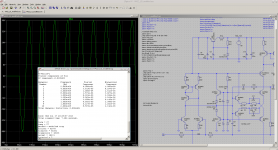
Using your asc file the amplifier shows a pretty good PM of about ~ 80 degree. GM is about 8 degree.
BR, Toni
Can't run fourier analysis as amplifier in this configuration using my zener lib is oscillating. Are you able to provide the part libraries too (used zeners ...)?Here it is, without the Cordell models. You may have to replace the diodes first, I haven't used your bx84 lib yet.
For sharing simulations using LTSpice it would be good if we could all use the same models...
BR, Toni
Code:
.model BZX84C3V0L D(Is=1.5n Rs=.5 Cjo=185p nbv=3 bv=3.0 Ibv=1m Vpk=3.0 mfg=OnSemi type=Zener)
.model BZX84C4V7L D(Is=1.5n Rs=.5 Cjo=185p nbv=3 bv=4.7 Ibv=1m Vpk=4.7 mfg=OnSemi type=Zener)
.model BZX84C5V1L D(Is=1.5n Rs=.5 Cjo=185p nbv=3 bv=5.1 Ibv=1m Vpk=5.1 mfg=OnSemi type=Zener)
.model BZX84C5V6L D(Is=1.5n Rs=.5 Cjo=185p nbv=3 bv=5.6 Ibv=1m Vpk=5.6 mfg=OnSemi type=Zener)
.model BZX84C6V2L D(Is=1.5n Rs=.5 Cjo=185p nbv=3 bv=6.2 Ibv=1m Vpk=6.2 mfg=OnSemi type=Zener)
.model BZX84C8V2L D(Is=.8n Rs=.5 Cjo=135p nbv=3 bv=8.2 Ibv=1m Vpk=8.2 mfg=OnSemi type=Zener)
.model BZX84C10L D(Is=.6n Rs=.5 Cjo=150p nbv=5 bv=10 Ibv=1m Vpk=10 mfg=OnSemi type=Zener)
.model BZX84C12L D(Is=.6n Rs=.5 Cjo=150p nbv=5 bv=12 Ibv=1m Vpk=12 mfg=OnSemi type=Zener)
.model BZX84C15L D(Is=.6n Rs=.5 Cjo=110p nbv=6 bv=15 Ibv=1m Vpk=15 mfg=OnSemi type=Zener)
.model BZX84C27L D(Is=.6n Rs=.5 Cjo=110p nbv=6 bv=27 Ibv=1m Vpk=27 mfg=OnSemi type=Zener)
.model BZX84C36L D(Is=.6n Rs=.5 Cjo=110p nbv=6 bv=36 Ibv=1m Vpk=36 mfg=OnSemi type=Zener)
.model BZX84C39L D(Is=.6n Rs=.5 Cjo=110p nbv=6 bv=39 Ibv=1m Vpk=39 mfg=OnSemi type=Zener)
.model BZX84C43L D(Is=.6n Rs=.5 Cjo=110p nbv=6 bv=43 Ibv=1m Vpk=43 mfg=OnSemi type=Zener)
.model BZX84C62L D(Is=.6n Rs=.5 Cjo=110p nbv=6 bv=62 Ibv=1m Vpk=62 mfg=OnSemi type=Zener)
.model BZX84C51L D(Is=.6n Rs=.5 Cjo=110p nbv=6 bv=51 Ibv=1m Vpk=51 mfg=OnSemi type=Zener)
.model BZX84C75L D(Is=.6n Rs=.5 Cjo=110p nbv=6 bv=75 Ibv=1m Vpk=75 mfg=OnSemi type=Zener)
.model BZX84C82L D(Is=.6n Rs=.5 Cjo=110p nbv=6 bv=82 Ibv=1m Vpk=82 mfg=OnSemi type=Zener)Wouldn't it be better for me to use the BZX84 library instead?
I tried this but then it's impossible to get it stable. There's too much gain and propagation delay to keep operating at a high frequency.Hi Guys
Instead of miller, have you tried comp from the VAS output back to the feedback summing node? To me, this would be intuitive given the inverting gain structure. This might require a further RC from VAS input to the +15V supply, or across the diff amp collectors.
I'm not sure whether they were conflicting - C31, the Cherry cap is a mandatory need to preserve stability and bandwidth and didn't have adverse effects on changing TMC values. It all depends on whether the VAS output or OPS output feedback is dominant with frequency.I'm sure you guys know better than I, but is it possible that the TMC and Cherry feedback might be in conflict coming back to the same point (VAS input)?
Have fun
Kevin O'Connor
However, now that I have my output inductor network, I learned that I could remove the TMC compensation completely and still retain stability for various capacitive loads. THD20K (100W/8Ohm) is 0.000038% now. I think that's as best as I can get it without compromizing stability further.
I'm sure dadod's output stage is more advanced and performs better than this MOSFET OPS. Perhaps there's some to gain there
Last edited:
...
Wouldn't it be better for me to use the BZX84 library instead?
Maybe - I have generated the "bzx84.lib" from single NXP models...
Can you confirm that your asc file from post #158 is stable to run a 20kHz fourier?
BR, Toni
Found the problem - a simple naming error. Now all sims are working correctly.Yeah it is. You mean the FFT you get when you choose the menu item "FFT" in the plotwindow after running a transient?
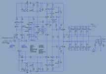
Attached is your original schematic with some added functions.
The label "x" at output has been moved back to the tianprobe junctions and the label "output" marks now the speaker output.
A quick THD20k@100W@8R shows:
Total Harmonic Distortion: 0.000640%
Think it's now time for you to create a prototype to verify simulations.
BR, Toni
Attachments
Yeah I had placed back the 'x' label in my schematic too, it got moved when I added the output filter.
It really depends on the amounts of compensation what the THD will be. It can range from sub-ppm to horrific 0.1% THD.
When trying to strike a balance between stability and THD, I end up with similar numbers. I've come to the conclusion that the TMC network is mandatory to iron out instabilities with certain C loads. However, I'm not letting the TMC dominate much over the Cherry feedback less THD goes down the drain again.
I should try the circuit with a different OPS. Either faster mosfets or move to a BJT output stage.
Suspect BJTs will provide lower THD.
Have you tried a diamond triple MOSFET output? I found it gives good results in simulation.
I haven't tried it yet, you have a reference on how to implement this? I suspect BJTs can yield lower THD. The annoying thing with MOSFET OPS is the severe Vgs modulation that the VAS has to cope with. I would guess Vbe modulation would be significantly less. (Vgs can go up a number of volts with decent output currents).
Edit: I searched Mouser, looking under 'e' to find ideal OPS blocks but no luck
Last edited:
If you are impatient I use a diamond stage in my attempt at amplifier design number 2. You could copy from there. But If you can wait I'll post up an .asc on that thread after work then you could graft the whole output stage onto your VAS.
Edit: My updated version of the diamond buffer can be configured to not use these devices the A1381/C3503 devices.
Edit: My updated version of the diamond buffer can be configured to not use these devices the A1381/C3503 devices.
Last edited:
I haven't tried it yet, you have a reference on how to implement this? I suspect BJTs can yield lower THD. The annoying thing with MOSFET OPS is the severe Vgs modulation that the VAS has to cope with. I would guess Vbe modulation would be significantly less. (Vgs can go up a number of volts with decent output currents).
Edit: I searched Mouser, looking under 'e' to find ideal OPS blocks but no luck
Try this HEC OPS http://www.diyaudio.com/forums/solid-state/238252-odnf-no-gnfb-power-amp-6.html#post3550195
Thank you both of you guys for sharing your work with me It'll be interesting to see how the different output stages will work out. I'll start working on that later today.
Meanwhile I've been tinkering with the compensation networks some more (this stuff can keep you busy for hours lol) and now came up with a version that retains stability with a much less drastic impact on THD, which is now 0.000070% for the schematic posted.
It drops TMC for TPC which, in combination with the Cherry cap (that mostly keeps phase in check) seems to work pretty well. I've added LG plots for the different compensations and then combines them. All tests were done with a 100nF zero R cap. I don't think I can get it much better
Well. Time to try a different OPS and see how that goes!
It'll be interesting to see how the different output stages will work out. I'll start working on that later today.Meanwhile I've been tinkering with the compensation networks some more (this stuff can keep you busy for hours lol) and now came up with a version that retains stability with a much less drastic impact on THD, which is now 0.000070% for the schematic posted.
It drops TMC for TPC which, in combination with the Cherry cap (that mostly keeps phase in check) seems to work pretty well. I've added LG plots for the different compensations and then combines them. All tests were done with a 100nF zero R cap. I don't think I can get it much better
Well. Time to try a different OPS and see how that goes!
Attachments
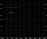
Have you checked PM? It seems to be very very low. About 7 degree ......
Meanwhile I've been tinkering with the compensation networks some more (this stuff can keep you busy for hours lol) and now came up with a version that retains stability with a much less drastic impact on THD, which is now 0.000070% for the schematic posted.
...
Meanwhile I've been tinkering with the compensation networks some more (this stuff can keep you busy for hours lol) and now came up with a version
I know what you mean about the compensation. It is critical to get it right giving the right balance between GM/PM/THD. I have spent many hours trying different things myself. I like TMC + Shunt compensation myself.
I will isolate my version of the x triple output stage and change the mosfet models to the same ones as you use (Bob Cordell's) to make it an easy copy and paste job. Will post it in this later on.
Paul
Last edited:
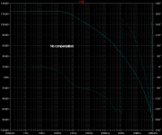
The last graph is -157 degrees through 0dB, with this illusive 100n and 0 ESR cap as load. No matter how I modify loads, I can't make it unstable by looking at the LG with various loads (that is, have a -180 degrees turn before 0dB where OLG=CLG. I'm not sure if that qualifies as stable-in-practiceHave you checked PM? It seems to be very very low. About 7 degree ...
For amplifier design I would recommend PM about 60 degree and GM > 6 dB. The absolutely minimum for PM should be > 45 degree.The last graph is -157 degrees through 0dB, with this illusive 100n and 0 ESR cap as load. No matter how I modify loads, I can't make it unstable by looking at the LG with various loads (that is, have a -180 degrees turn before 0dB where OLG=CLG. I'm not sure if that qualifies as stable-in-practice
BTW would it be possible for you to provide the latest asc (
) as after adding your new tpc values I have simulated only 7 degree PM which is not the same as your values. Maybe I have overlooked a new/changed value ...Just to be sure: I am running LTSpice 4.18m from 2013.07.13
BR, Toni
Thanks! overlooked R5/R6 changes... forgive a blind old man ...Okies, here's the .asc file.
- Status
- This old topic is closed. If you want to reopen this topic, contact a moderator using the "Report Post" button.
- Home
- Amplifiers
- Solid State
- My New VAS Topology