You know the answer to this. But for those who perhaps don't.
For one, consider the intensity of magnetic field induction around power components. As currents rise so do the intensity of the field around them.
Sticking a trace and a half turn inductor created by a via under a power component is bad news.
The inductance created from trace length is small and I believe is more a linear relationship. However the intensity of a magnetic field follows inverse square law. For ever doubling of distance between components the magnetic field intensity drops by the square of the distance.
The same distance-intensity relationship holds true for voltage fields as well.
Therefore EM and EMI is an inverse square law relationship.
The only reason high density PCB designs are used is to save cost. EEs are under a lot pressure to reduce the physical size of products to remain competitive not because it better. Products used to be a lot bigger and take up a lot more space. There is a reason for that.
Distance between components is your friend. Longer traces and greater distance between traces are not a bad thing.
Last but certainly not least, Using large plains on multi layer boards requires a lot know how. Consider a simple double sided board. If you where place a ground plane on both sides of the board you have created a dipole antenna and this is a recipe for EMI and RF interference. The same holds true for ground planes and power planes, Why? because for AC signals there is no distinction between type of planes.
This is basic high school physics.
The average DIYer simply doesn't have the knowledge and experience to do multi layer multi plane PCB design. I certainly don't.
And why are we considering taking from publications for high speed data and RF PCB routing design and applying it audio?
Douglas please correct any errors in this.
@AndriyOL
For you I suggest sticking to the simplest of PCB design. No more than double sided. If you are going to use a ground plane then keep it on the component side
and put as much of the trace on the bottom as possible. Use the top to replace what would otherwise be wire jumpers connecting bottom traces.
Space you components out more and don't run trace or place vias underneath components. Do not run trace through pads that connect paralleled components. Instead run a single trace and tap off of that.
Avoid putting ground plane anywhere near the output stage of pre-driver. Doing this would only couple the high current output stage to the input stage. You want your ground potential to the same. A strong field from the output cutting through a ground plane will change the potential. That alone could cause oscillations.
If this design requires a multi plane, multi layer board just to get it going then there is something fundamentally wrong with the circuit design.
I'm sure that statement will flame a few egos.
A monkey see monkey do approach to audio PCB design won't work.
Keep it simple.
As far as I know, the longer the traces the bigger inductance and rf noise acceptance. All these limits GBW and make the circuit more prone to oscillation.
I agree that components crowding isn't pleasing for an eye, but wiring crowd isn't pleasing for the signal.
I only plan to place one gnd plane between both sides of input part of the pcb, closer to bottom side, where the most of wiring is.
Perhaps because of audio become more like rf wise.
I agree that components crowding isn't pleasing for an eye, but wiring crowd isn't pleasing for the signal.
I only plan to place one gnd plane between both sides of input part of the pcb, closer to bottom side, where the most of wiring is.
Perhaps because of audio become more like rf wise.
Last edited:
I agree with you David, the design should work on double sided pcb, but if I made a serious fault in layout it may not work at all.
As have been said by xx3stksm, multi-layer pcb outperform double-layer in almost every way.
I use high density pcb because of limited heatsink space.
I also guess the rf ingress can get into amplifier via psu and it's wiring as well. So, the best is to place in metal enclosure all the amp and psu units. When I make the case I'll do it.
Last edited:
For what muli layer PCB are intended for, high speed data and microwave, they do. But for audio they are not needed and if it makes that big a difference for audio circuits then there is something fundamentally wrong.
None of this has been a requirement for audio over the last 40 years and more.
I would rather take the advice from an experienced electrical engineer who's been designing audio power for I'm guessing over 40 years.
If you disagree then I guess you live with your problems.
None of this has been a requirement for audio over the last 40 years and more.
I would rather take the advice from an experienced electrical engineer who's been designing audio power for I'm guessing over 40 years.
If you disagree then I guess you live with your problems.
Everyone has their standard which is not usually explained in detail. Mine is simple. The ground potential must be equal wherever you connect a scope. But this is almost impossible in a power amplifier because 16 volts(8 ohms load) means 4 amperes peak to peak which ends up 0.1 volt(0.025 ohm ground resistance). 0.1 volt is not acceptable.
I use class A BTL which doesn't have current flow into the signal ground. Current flow is through both power rails only. Furthermore, class A decreases alternating current from power rails practically by 40dB. So, current flow into the ground plane is almost ignorable, and power planes are 4/100=0.04 ampere in my circumstance.
But I still use ground plane because I need a digital circuit for temperature monitor, bias current control, short circuit protection, and DC offset control. I'm sure a power amplifier must have such monitor system to prevent it from a various dangerous situation. I know many people dislike a digital monitoring system in an audio system because it uses digital ICs which tends to make digital noise.
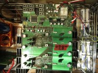
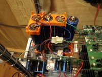
That's why I need a multi-layer PCB which has ground plane and far better noise immunity than two-layer. I don't need a multi-layer PCB for an RIAA equalizer because it has no digital stuff at all. A digital monitoring system is very effective than an ordinary analog one. The disadvantage is digital noise caused by poor ground routing. My solution to a power amplifier is class A BTL and a digital monitoring system realized by a multi-layer PCB. I usually forget to explain the former and say the conclusion only; a multi-layer is better. What I mean is of course both. The pics are my power amplifier designed by this concept. One more thing I forgot is mine has DAC on the board. The reason is to prevent common mode current problem caused by the mains. This is off the thread.
I use class A BTL which doesn't have current flow into the signal ground. Current flow is through both power rails only. Furthermore, class A decreases alternating current from power rails practically by 40dB. So, current flow into the ground plane is almost ignorable, and power planes are 4/100=0.04 ampere in my circumstance.
But I still use ground plane because I need a digital circuit for temperature monitor, bias current control, short circuit protection, and DC offset control. I'm sure a power amplifier must have such monitor system to prevent it from a various dangerous situation. I know many people dislike a digital monitoring system in an audio system because it uses digital ICs which tends to make digital noise.
That's why I need a multi-layer PCB which has ground plane and far better noise immunity than two-layer. I don't need a multi-layer PCB for an RIAA equalizer because it has no digital stuff at all. A digital monitoring system is very effective than an ordinary analog one. The disadvantage is digital noise caused by poor ground routing. My solution to a power amplifier is class A BTL and a digital monitoring system realized by a multi-layer PCB. I usually forget to explain the former and say the conclusion only; a multi-layer is better. What I mean is of course both. The pics are my power amplifier designed by this concept. One more thing I forgot is mine has DAC on the board. The reason is to prevent common mode current problem caused by the mains. This is off the thread.
Attachments
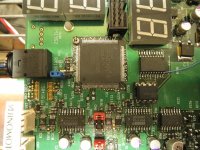
I can't help but notice from the pics of PCB that board look very contaminated with bits of solder. The soldering look rough with usually means it cold. <snip>
Have a look at the density of some of today's designs... shortest route is always best, thermal issues can be easily managed by good design. Larger power boards you obviously have to have some space around power components and inductors, but digital you can cram it in, often there is no space between components what so ever. It depends on the design at the end of the day.
Concise tight blocks of related circuitry, with power islands, inter block separation is the best way.
Routing under components, effect can vary, never route under magnetic components, ever, as to the rest it depends on size, what signal they are carrying etc. often you have too, to avoid large loops, especially op-amp feedback loops.
A muli-layer digital or digital/sensitive analogue board with multiple ground planes, multiple signal layers is a totally different beast to a high power output board, that said a lot of automotive stuff due to space restrictions is a mixture of both... as are other designs, flexi rigid with 20+ PTH TO-220 FETs on a bespoke heatsink and the same number of TO-263 devices using thermal vias and multiple 2oz flex layers to dissipate and spread the heat.
For what muli layer PCB are intended for, high speed data and microwave, they do. But for audio they are not needed and if it makes that big a difference for audio circuits then there is something fundamentally wrong. <snip>
For low level analogue a multi layer is always best choice, 4 can often suffice for a simple analogue circuit.
For a simple power section I have always preferred bus bar routing (broadside couples power track and its return) using the correct track width for the current capacity. This contains and limits the magnetic interference this high power tracks will have on the surrounding circuitry. Depending on the complexity and requirements though done power amps from 2 to 8 layers, each circuit is different and requires the best solution (this is a wide range of power amps).
As for digital every board I have ever worked on we have worked to limit loop length of signals, to minimise signal integrity/EMC issues. Crosstalk, noise pickup all get worse with long signal runs, as does HF losses on the often fast rise time signal, pr emphasis on the signal can be avoided. Also shorter signals are less effected by reflections... A famous rule has always been the 1ns rule, if a signal has a rise time of 1ns any length over 3 inch will be prone to reflections bouncing back to the transmitter before the signal has finished it full rise from 0V to whatever level it goes to.
From that you can see that a 1ns rise time is about 6" long...
A famous rule has always been the 1ns rule, if a signal has a rise time of 1ns any length over 3 inch will be prone to reflections bouncing back to the transmitter before the signal has finished it full rise from 0V to whatever level it goes to.
From that you can see that a 1ns rise time is about 6" long...
What can you say about my pcb layout and schematic Marce, why the amp is oscillating?
But I still use ground plane because I need a digital circuit for temperature monitor, bias current control, short circuit protection, and DC offset control. I'm sure a power amplifier must have such monitor system to prevent it from a various dangerous situation. I know many people dislike a digital monitoring system in an audio system because it uses digital ICs which tends to make digital noise.
.
It's worth pointing out that all of those functions can be easily carried out with analogue circuitry, and in the absence of anything more complicated that would be the route I would normally take.
However, sometimes you really need a microcontroller, say for decoding RC-5 IR commands. This is accepted reluctantly because it adds another level of complexity, introduces software control issues, and threatens digital noise.
But... I have designed many preamps and power amps for production that had a microcontroller, and in no case was digital noise measurable. All the PCBs were 2-layer.
Far be it from me to say 4-layer is never required. But for me it comes in with tightly packed SMT analogue PCBs where you need at least one more layer for routing. If that's sufficient the remaining layer will very likely be set as a ground plane, to reduce ground resistance and so reduce inter-channel crosstalk.
Reasons Of Oscillations In Audio Amplifiers And Best Ways Of Elimination
Straight or compensation?
What was measurement threshold?
Powerful AB OPS have at least three meaningful impacts to the small-signal circuitry.
1. Through supply rails and/or shared trafo/mains
2. Through common ground or dedicated common point
3. Through inductive/capacitive influences between signal tracks
Douglas, what was the measurenent method?But... I have designed many preamps and power amps for production that had a microcontroller, and in no case was digital noise measurable. All the PCBs were 2-layer.
Straight or compensation?
What was measurement threshold?
This is truly depends of unity gain frequency, mode of operation and desired dynamical range.Far be it from me to say 4-layer is never required. But for me it comes in with tightly packed SMT analogue PCBs where you need at least one more layer for routing.
Powerful AB OPS have at least three meaningful impacts to the small-signal circuitry.
1. Through supply rails and/or shared trafo/mains
2. Through common ground or dedicated common point
3. Through inductive/capacitive influences between signal tracks
Powerful AB OPS have at least three meaningful impacts to the small-signal circuitry.
1. Through supply rails and/or shared trafo/mains
2. Through common ground or dedicated common point
If I have a separate PSUs for small-signal circuitry and OPS, should I use common GND for both PSUs or separate GNDs for OPS and small-signal circuitry? Currently they are separated via 10R resistor.
AndriyOL,
I suppose the best person to help you is Lazy Cat as he is the project owner and have total control of this project concept.
So Lazy Cat is the designer? Certainly he should have some helpful info.
I don't think it's been confirmed yet if the amplifier is currently capable of driving sinewaves into a load? Is it?
Yes, he is the designer of basic schematic, one of which is shown in post 51 for example.
Do you mean at full power? I only tried to play music with 50-80 watts I think but with minimum ops bias current.
Could someone advise how to calibrate HF compensation in the amp that the phase margin won't colide with OLG?
Do you mean at full power? I only tried to play music with 50-80 watts I think but with minimum ops bias current.
Could someone advise how to calibrate HF compensation in the amp that the phase margin won't colide with OLG?
Last edited:
Standard audio measuring techniques using Audio Precision, and full EMC emissions approval testingDouglas, what was the measurenent method?
I have no idea what this means.Straight or compensation?
Varying in each case, depending on the noise floor. You will appreciate it would not be appropriate for me to share the test results with you.What was measurement threshold?
- Home
- Amplifiers
- Solid State
- One of the Top Solid-State CFA amp design