Hi all,
I have for some time now been trying to set up a realistic ADC/DAC PSU decoupling capacitor LTSpice simulation model that will give a quite realistic impression of what a given selection of decoupling capacitors will look like electrically.
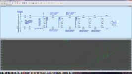
I have attached a copy of the model I currently use (based on Saturn PCB Design toolkit estimations for trace inductance, - etc.), however, I am unsure as to how to model the internals of the ADC/DAC itself ... ?
Also, when modeling the DAC/ADC power draw as a variable current source, it looks as if the damping brought about by the decoupling capacitors is quite limited - only - 24 dB at lower frequencies and already at ~ 13.5 MHz the attenuation is 0 dB.
I reckon something is amiss here and it would be great to actually have a simulation model that can be considered realistic. Thus, if you have any experience with - roughly - simulating ADC/DAC decoupling capacitor network I'd appreciate your input.
BTW the attached simulation model's DAC pin specs are based on the distant wires (from pin 1, 14, 15, 28 to internal silicon) of an 28 pin SSOP package.
Cheers & have a good day,
Jesper
I have for some time now been trying to set up a realistic ADC/DAC PSU decoupling capacitor LTSpice simulation model that will give a quite realistic impression of what a given selection of decoupling capacitors will look like electrically.
I have attached a copy of the model I currently use (based on Saturn PCB Design toolkit estimations for trace inductance, - etc.), however, I am unsure as to how to model the internals of the ADC/DAC itself ... ?
Also, when modeling the DAC/ADC power draw as a variable current source, it looks as if the damping brought about by the decoupling capacitors is quite limited - only - 24 dB at lower frequencies and already at ~ 13.5 MHz the attenuation is 0 dB.
I reckon something is amiss here and it would be great to actually have a simulation model that can be considered realistic. Thus, if you have any experience with - roughly - simulating ADC/DAC decoupling capacitor network I'd appreciate your input.
BTW the attached simulation model's DAC pin specs are based on the distant wires (from pin 1, 14, 15, 28 to internal silicon) of an 28 pin SSOP package.
Cheers & have a good day,
Jesper
Attachments
Just two comments, neither of which answers your question:
1. Regulator outputs are normally quite inductive. That's due to the loop gain of the control loop falling with frequency.
2. Murata has some very extensive lumped models for their capacitors on their website. They don't include the capacitance reduction with non-zero DC voltages of class 2 ceramic capacitors as far as I know, but all the resistive and inductive effects are included. The schematics are complicated and poorly readable, so I guess they are automatically generated from measured s-parameter data.
Hi Marcel ... well, thanks for your feedback although, as you write, it doesn't really solve the "challenge" with simulating this realistically. Even with better models I reckon that this basic simulation model's shift from decoupling to "amplifying" the noise at 13.5 MHz would still be there - and I just doubt (hope?) that this is the way it is (supposed to be) ...
When searching the literature and recommendations for decoupling it seems that there are two main approaches to this:
1. To use one or more capacitors with the same value ideally selected to have the lowest impedance at the fundamental/base frequency of the circuitry PSU "noise", i.e. for a DAC with a sampling frequency of 192 kHz (12.** MHz clock) then a possibly feasible choice could be the ubiquitous 100 nF capacitor.
2. To use more capacitors of different values to decouple the circuitry at different frequencies - optimally to achieve an equal impedance throughout the relevant frequency spectrum. This is what I have tried to simulate in the simulation above with (I reckon) quite realistic values for inter-capacitor trace inductances etc.
The basic issue I suppose is that whereas approach 1. may filter the base frequency (100 nF has an impedance low at ~ 12 MHz) then it is relatively inefficient at higher frequencies - where the PSRR of the typical ICs also drops. Meaning that a good portion of the higher harmonics of the digital signals related to an IC ADC/DAC may only be partially decoupled.
Approach 2 might be more efficient at filtering a wider range of frequencies, however, if the decoupling/amplifying point is at ~ 13.5 MHz I suppose something is not correct with the model.
I could & do build test circuits but it would just be so much simpler to be able to simulate potential solutions without the building phase ... And to this end have a simulation model that realistically models what the damping would be a different frequencies ...
Are there no others here on diyaudio that have considered this to be a challenge/an issue - and have tried to realistically model a solution? Or might I be missing something here ... ?
Cheers,
Jesper
Last edited:
Apart from the regulator, I think the main weakness in the model is the frequency-independent ESR of the capacitors. That would correspond to a tan(delta) that is proportional to frequency, but capacitor datasheets often show a tan(delta) that is nearly frequency independent. Besides, if the reference and its return are on adjacent IC package pins, you would normally get a coupling factor of about 0.5 between their inductances.
Nevertheless, it is true that capacitors in parallel with wires in between can go into parallel resonance.
Nevertheless, it is true that capacitors in parallel with wires in between can go into parallel resonance.
Hi & good morning to you both ... Well, I/we actually just came out of a weekend where we've had a hurricane pass over Denmark with wind speeds reaching 40 m/s (aka 144 km/h !). Somewhat humbling to experience such an unabated wind & nature at full (?) force ... Fortunately no major personal harm done but since Denmark is a sea-near country there are many people facing real challenges when the sea level rises (more than) two meters above normal reference level ...
Anyway, returning to the subject ...
@phase: Yes, there would be capacitors both near the LDO & the DAC chip - and here assuming where you are heading with your question ... that may add some inductance to the trace from the LDO to the capacitors, and an additional capacitor (e.g. 4.7uF with an LT3042). However, it doesn't really change things as seen from the DAC perspective as far as I can see, i.e. V2_P & V1_N & V2_P simulation values are very close to being the same. Did you have something particular in mind?
@MarcelvdG: Thanks again, Marcel, for your feedback. A little bit puzzled by parts of it, though ...
https://ksim3.kemet.com/capacitor-simulation
From a practical perspective I have also been considering ways of measuring this in an actual circuitry. One way of doing this could be to observe the noise spectrum of a DAC PSU line in use with a wide-band spectrum analyzer. This likely would show a non-discerning combination of the noise generated by the decoupling network's impedance non-linearities and the DAC's intrinsic workings.
Another way might be to use something like a VNA to get an impedance vs. frequency profile for the decoupling network being considered. Which sounds attractive, however, I am just a little unsure of the practical resolution of a VNA at low impedances - thus, would it be able to unveil impedance variations as low as maybe +/- 10 mohms at a 20 mohm base level? And would using a VNA at all be relevant in terms of telling something about the decoupling network in combination with the DAC/ADC?
Well, many thoughts here ... I'd appreciate your feedback or thoughts on this as you or others feel inclined to ...
Cheers & have a good day,
Jesper
Anyway, returning to the subject ...
@phase: Yes, there would be capacitors both near the LDO & the DAC chip - and here assuming where you are heading with your question ... that may add some inductance to the trace from the LDO to the capacitors, and an additional capacitor (e.g. 4.7uF with an LT3042). However, it doesn't really change things as seen from the DAC perspective as far as I can see, i.e. V2_P & V1_N & V2_P simulation values are very close to being the same. Did you have something particular in mind?
@MarcelvdG: Thanks again, Marcel, for your feedback. A little bit puzzled by parts of it, though ...
Referencing a capacitor data sheet (that I would consider relevant in my context) I notice that KEMET only specifies tan(delta) at 1 kHz for sizes greater than 1nF - at least in this datasheet. That would be a less than useful specification unless there is a reliable way to extrapolate this value to higher frequencies ... here I am thinking that it would be feasible to get an idea about how much the influence of tan(delta) actually is in a particular situation .. Thus, would you happen to know e.g. what the tan(delta) for a 100 nF C0G 1210 capacitor is at, say, 25 MHz (or another capacitor you know of)? Also, to this end, would you think that the tan(delta) aspect is included in a simulation tool like this one from KEMET:That would correspond to a tan(delta) that is proportional to frequency, but capacitor datasheets often show a tan(delta) that is nearly frequency independent.
https://ksim3.kemet.com/capacitor-simulation
If I understand you correctly - if you have two adjacent pins, e.g. VCC and its GND return placed adjacent to eachother - then the combined inductance would not be the added inductance of the two pins but the added inductance multiplied by 0.5. Is that correctly understood? If so, then it is quite huge actually since it would shift the optimum decoupling capacitor a couple of values for the same (higher) frequency .. !! Now, I realize that you are very well versed in engineering theory, but are you sure about this? I've never seen it mentioned anywhere ....Besides, if the reference and its return are on adjacent IC package pins, you would normally get a coupling factor of about 0.5 between their inductances.
Hmmm ... just wondering what you are talking about here: are you referring to what could also be called the "anti-resonance" behavior of a capacitor (seen as dips and peaks in the simulation in post #1 for different values of adjacent capacitors), or may you be referring to something else?Nevertheless, it is true that capacitors in parallel with wires in between can go into parallel resonance.
From a practical perspective I have also been considering ways of measuring this in an actual circuitry. One way of doing this could be to observe the noise spectrum of a DAC PSU line in use with a wide-band spectrum analyzer. This likely would show a non-discerning combination of the noise generated by the decoupling network's impedance non-linearities and the DAC's intrinsic workings.
Another way might be to use something like a VNA to get an impedance vs. frequency profile for the decoupling network being considered. Which sounds attractive, however, I am just a little unsure of the practical resolution of a VNA at low impedances - thus, would it be able to unveil impedance variations as low as maybe +/- 10 mohms at a 20 mohm base level? And would using a VNA at all be relevant in terms of telling something about the decoupling network in combination with the DAC/ADC?
Well, many thoughts here ... I'd appreciate your feedback or thoughts on this as you or others feel inclined to ...
Cheers & have a good day,
Jesper
Regarding tan(delta), it depends on what frequency range you look at. In that KEMET tool, you see the ESR drop more or less proportionally with the capacitive reactance (near constant tan(delta)) until it becomes more or less flat (constant ESR). If your resonances are all in the constant ESR frequency range, then my comment doesn't apply.

With parallel resonance, I indeed meant the impedance peaks.
Regarding the coupling factor: you understood exactly what I meant. I have designed integrated circuits for about two and a half decades and we usually get a large file with inductances and mutual inductances (among other things) to model the package. Wirebond packages with a lead frame typically have a coupling factor of the order of 0.5 between adjacent pins (lead frame + bond wire), although the exact value depends on the precise package and the pin numbers.
I was just wondering if there were two parts, or if it had been intended for one to accomplish both reg output, and decoupling.
I see data sheets that recommend the use of a tantalum, and the only reason I can think of is that they have a flat impedance curve. Handy, since it’ll work in a a variety of layout situations, but never liked the way they sounded.
I see data sheets that recommend the use of a tantalum, and the only reason I can think of is that they have a flat impedance curve. Handy, since it’ll work in a a variety of layout situations, but never liked the way they sounded.
Hi & thank you both for considering & giving feedback ")
@phase: It sort of is a combined simulation model hopefully considering both ends of the electron supply chain - the (likely) LDO and then what is in-between until reaching the DAC/ADC. However, I've found that what matters most in terms of resonances etc. are the components placed adjacent to the DAC/ADC (or rather simultaneous low(er) values of capacitance, inductance & impedances). This may be obvious if considering a mathematical model but nevertheless has been quite frustrating since trying to reach low decoupling capacitor impedance values appears to almost imply high Q effects. Which on the other hand does not support an even decoupling capacitor impedance curve wrt frequency. So, at least to me, it is kind of a neverending story to find feasible & balanced solutions ...
Which actually is why I posted the model above - by doing so I was really hoping to find "serious" flaws in it, and thus, have renewed hope that the very low impedances of e.g. C0G capacitors could be unquestionably beneficial ... But if I read Marcel's replies correctly adding the tan(delta) variation with frequency and the LDO inductance variation with frequency will change things - but not "significantly" so, i.e. overall the simulation will look similar ...
WRT tantalum capacitors to my memory Cyril Bateman in his capacitor distortion tests found that they were hugely distorting so I have never really considered them.
I did, however, try one slightly different simulation yesterday and that was to substitute the values of inductance, impedance & capacitance in the simulation model above for WIMA FKP2 & FKP02 values. And doing so leads to a much more even impedance curve in the higher frequencies (and it might also sound better, who knows). Obviously, the physical sizes of these capacitors are much larger than SMD capacitor sizes but the inductances of power planes - or wide traces over a closely placed GND plane - is rather low (~ 0.1 nH/mm for a 2mm wide trace with a 0.25mm GND plane to trace spacing) so that these capacitors' PCM5 or PCM2.5 pin spacings are not too problematic.
I think it's worth a try to see what the PSU line noise spectra of both solutions (SMD C0G vs PP capacitors) look like.
@MarcelvdG: Hmmm ... thanks again for your reply, Marcel - as always very good feedback. I'll reply sort of in reverse order ...
Since we have "met" before here on diyaudio, and I have found your replies to be very insightful (and educating), I actually have been wondering what your occupation was (or used to be) ... And although I admittedly do not have any real knowledge of IC design, I reckon it nevertheless requires a very good theoretical and practical understanding of engineering. And, also admittedly, reading that you have such experience many questions popped up on topics that I suppose you would know about. But I'll leave it be - just fine to know (part of) where you come from in a professional perspective.
One question though which I would appreciate your feedback on: I have been trying to find reliable sources on how to layout analog signal PCBs in ways that allow for least interference between circuitry "blocks". I.e. how to avoid that "the least resistance" of currents causes bleeds into adjacent circuitry blocks while keeping an unbroken ground plane (or GND traces), and low EMI radiation both externally and internally in the circuitry. There are books by Lee Ritchey, Howard Johnson, Henry Ott, and maybe Bruce Archambeault - but most of these appear to be focused on digital signals where, well, things are different. I have not really found any books/papers with hands-on examples outlining best practices for very low noise analog circuitry PCB layout ... I.e. how to optimally place rectifying diodes, radiation from components, ground plane or not, distances needed to achieve ** dB of damping, the need/benefits of shielding, etc. ...
A practical current challenge is a low noise linear power supply where the LTSpice simulation gives an ~-140 dB damping of AC input noise at DC which drops to ~-190 dB at 100 Hz. However, when measuring the actual circuitry the ~DC level is around - 110 dB, 100 Hz is around - 140 dB, and then the circuitry noise vanishes into the measurement setup noise level just a bit above 100 Hz (~- 150 dB). I really would like to reach the -140 dB level - and in the process of doing so learn what the thinking behind doing so is.
Would you happen to know about "a book" or paper(s) that describes how & not least why some analog circuitry PCB layout approaches work? As I reckon you know I am not as theoretically founded as you are but I have a quite good understanding of concepts and particularly hands-on examples.
Regarding the capacitor models I think that most of the SMD capacitors I consider using will be in the constant ESR region for the relevant frequencies. However, for the larger value (electrolytic) capacitors this will not be the case. So I reckon it would be relevant to include the frequency variant tan(delta) addition here ... While saying so I am also thinking that the practical amplitude level of high frequencies reaching these larger capacitors will be relatively low as such frequencies have been filtered by the SMD capacitors?
As it is I have ordered a selection of capacitors and will try to measure how PSU noise varies with capacitor size & value in the circuitry in question. Would be great if the simulation model actually appears to show some resemblance to reality ...
Cheers,
Jesper
@phase: It sort of is a combined simulation model hopefully considering both ends of the electron supply chain - the (likely) LDO and then what is in-between until reaching the DAC/ADC. However, I've found that what matters most in terms of resonances etc. are the components placed adjacent to the DAC/ADC (or rather simultaneous low(er) values of capacitance, inductance & impedances). This may be obvious if considering a mathematical model but nevertheless has been quite frustrating since trying to reach low decoupling capacitor impedance values appears to almost imply high Q effects. Which on the other hand does not support an even decoupling capacitor impedance curve wrt frequency. So, at least to me, it is kind of a neverending story to find feasible & balanced solutions ...
Which actually is why I posted the model above - by doing so I was really hoping to find "serious" flaws in it, and thus, have renewed hope that the very low impedances of e.g. C0G capacitors could be unquestionably beneficial ... But if I read Marcel's replies correctly adding the tan(delta) variation with frequency and the LDO inductance variation with frequency will change things - but not "significantly" so, i.e. overall the simulation will look similar ...
WRT tantalum capacitors to my memory Cyril Bateman in his capacitor distortion tests found that they were hugely distorting so I have never really considered them.
I did, however, try one slightly different simulation yesterday and that was to substitute the values of inductance, impedance & capacitance in the simulation model above for WIMA FKP2 & FKP02 values. And doing so leads to a much more even impedance curve in the higher frequencies (and it might also sound better, who knows). Obviously, the physical sizes of these capacitors are much larger than SMD capacitor sizes but the inductances of power planes - or wide traces over a closely placed GND plane - is rather low (~ 0.1 nH/mm for a 2mm wide trace with a 0.25mm GND plane to trace spacing) so that these capacitors' PCM5 or PCM2.5 pin spacings are not too problematic.
I think it's worth a try to see what the PSU line noise spectra of both solutions (SMD C0G vs PP capacitors) look like.
@MarcelvdG: Hmmm ... thanks again for your reply, Marcel - as always very good feedback. I'll reply sort of in reverse order ...
I have designed integrated circuits for about two and a half decades
Since we have "met" before here on diyaudio, and I have found your replies to be very insightful (and educating
), I actually have been wondering what your occupation was (or used to be) ... And although I admittedly do not have any real knowledge of IC design, I reckon it nevertheless requires a very good theoretical and practical understanding of engineering. And, also admittedly, reading that you have such experience many questions popped up on topics that I suppose you would know about. But I'll leave it be - just fine to know (part of) where you come from in a professional perspective.One question though which I would appreciate your feedback on: I have been trying to find reliable sources on how to layout analog signal PCBs in ways that allow for least interference between circuitry "blocks". I.e. how to avoid that "the least resistance" of currents causes bleeds into adjacent circuitry blocks while keeping an unbroken ground plane (or GND traces), and low EMI radiation both externally and internally in the circuitry. There are books by Lee Ritchey, Howard Johnson, Henry Ott, and maybe Bruce Archambeault - but most of these appear to be focused on digital signals where, well, things are different. I have not really found any books/papers with hands-on examples outlining best practices for very low noise analog circuitry PCB layout ... I.e. how to optimally place rectifying diodes, radiation from components, ground plane or not, distances needed to achieve ** dB of damping, the need/benefits of shielding, etc. ...
A practical current challenge is a low noise linear power supply where the LTSpice simulation gives an ~-140 dB damping of AC input noise at DC which drops to ~-190 dB at 100 Hz. However, when measuring the actual circuitry the ~DC level is around - 110 dB, 100 Hz is around - 140 dB, and then the circuitry noise vanishes into the measurement setup noise level just a bit above 100 Hz (~- 150 dB). I really would like to reach the -140 dB level - and in the process of doing so learn what the thinking behind doing so is.
Would you happen to know about "a book" or paper(s) that describes how & not least why some analog circuitry PCB layout approaches work? As I reckon you know I am not as theoretically founded as you are but I have a quite good understanding of concepts and particularly hands-on examples.
Regarding the capacitor models I think that most of the SMD capacitors I consider using will be in the constant ESR region for the relevant frequencies. However, for the larger value (electrolytic) capacitors this will not be the case. So I reckon it would be relevant to include the frequency variant tan(delta) addition here ... While saying so I am also thinking that the practical amplitude level of high frequencies reaching these larger capacitors will be relatively low as such frequencies have been filtered by the SMD capacitors?
As it is I have ordered a selection of capacitors and will try to measure how PSU noise varies with capacitor size & value in the circuitry in question. Would be great if the simulation model actually appears to show some resemblance to reality
...Cheers,
Jesper
Empirically, 805 SMD film cap such as those made by Rubycon are good for bypass of some analog dac circuitry (including for some of analog RF). Good quality aluminum electrolytics can be used in parallel if needed (e.g., say, maybe Panasonic FC). Some problems with inductance can be reduced by avoiding vias in the bypass current path (i.e. consider routing bypass current on surface ground fill). For digital dac circuitry the conventional .1uf to .01uf X7R bypass cap strategy seems to work fine. Of course YMMV. Also, doesn't hurt if using film caps (or C0G/NPO) for bypass to check for possible power rail ringing with a low capacitance active scope probe. Another thing that sometimes helps with dac analog power rails is to try loading them with a resistor to ground. Easy experiment to do, sometimes proves useful, other times not
Last edited:
One question though which I would appreciate your feedback on: I have been trying to find reliable sources on how to layout analog signal PCBs in ways that allow for least interference between circuitry "blocks". I.e. how to avoid that "the least resistance" of currents causes bleeds into adjacent circuitry blocks while keeping an unbroken ground plane (or GND traces), and low EMI radiation both externally and internally in the circuitry. There are books by Lee Ritchey, Howard Johnson, Henry Ott, and maybe Bruce Archambeault - but most of these appear to be focused on digital signals where, well, things are different. I have not really found any books/papers with hands-on examples outlining best practices for very low noise analog circuitry PCB layout ... I.e. how to optimally place rectifying diodes, radiation from components, ground plane or not, distances needed to achieve ** dB of damping, the need/benefits of shielding, etc. ...
A practical current challenge is a low noise linear power supply where the LTSpice simulation gives an ~-140 dB damping of AC input noise at DC which drops to ~-190 dB at 100 Hz. However, when measuring the actual circuitry the ~DC level is around - 110 dB, 100 Hz is around - 140 dB, and then the circuitry noise vanishes into the measurement setup noise level just a bit above 100 Hz (~- 150 dB). I really would like to reach the -140 dB level - and in the process of doing so learn what the thinking behind doing so is.
Would you happen to know about "a book" or paper(s) that describes how & not least why some analog circuitry PCB layout approaches work?
In the early 1990's, I learned a lot from the book Elektromagnetische compatibiliteit by J. J. Goedbloed (in Dutch, but also translated into English). I haven't a clue if what Goedbloed wrote isn't covered by the books you already read, though. The book is more practical than the title suggests.
At high frequencies, the return currents take the path of least flux and flow right below the signal conductor, as long as there is a plane to flow through. They spread out more at low frequencies, where resistance has more impact than inductive reactance. I probably should be able to calculate by how much if I were any good at electromagnetic field calculations, but I'm not.
Hi all - & thanks again for commenting & suggesting ...
@Markw4: Hmmm ... thanks for your feedback, Mark. I feel like just giving it a little time to "simmer" in my thoughts, so to speak, and then I may get back with more feedback/comments later. I'm currently making some test PCBs of the DAC I'm using (PCM1794 DDDAC variant) and will try to check e.g. for supply ringing.
@MarcelvdG:
@phase: Interesting observation ... Any chance you can say a bit about what the ringing looked like? In my thinking I suppose it could be related to the inductance (if visible on a scope?) - don't you think that the damping of the capacitor itself (i.e. inter-layer damping) would not be visible other than as some kind of distortion?
Cheers,
Jesper
@Markw4: Hmmm ... thanks for your feedback, Mark. I feel like just giving it a little time to "simmer" in my thoughts, so to speak, and then I may get back with more feedback/comments later. I'm currently making some test PCBs of the DAC I'm using (PCM1794 DDDAC variant) and will try to check e.g. for supply ringing.
@MarcelvdG:
Well, what do you know ...?? The Danish National libraries actually have this book in English so I have reserved it - could be that it covers matters from a different perspective than the ones I already know of. Thanks for the tip, Marcel!In the early 1990's, I learned a lot from the book Elektromagnetische compatibiliteit by J. J. Goedbloed
@phase: Interesting observation ... Any chance you can say a bit about what the ringing looked like? In my thinking I suppose it could be related to the inductance (if visible on a scope?) - don't you think that the damping of the capacitor itself (i.e. inter-layer damping) would not be visible other than as some kind of distortion?
Cheers,
Jesper
Ringing is presumably going to be dependent on an underdamped LCR circuit, plus some excitation. For example, with digital circuitry clock edges can kick a resonant circuit into damped ringing.
With analog circuitry there can sometimes be a different problem where a load exhibits some negative resistance allowing for possible oscillation with underdamped LCR bypass impedance as part of the tank circuit. Not that common a problem with audio opamps IME, although AD797 datasheet contains some application advice about possible need for damping larger electrolytics if too near the power pins.
Clock modules are some combination of analog and digital circuitry. Some of them can be sensitive to byapss cap types and or to the presence of ferrites intended for power rail isolation. I am guessing the issue with ferrites could be related to hysteresis noise/distortion, but have not tried to measure it.
Last edited:
@Markw4: Hi again Mark ... I think it is time to give a bit of feedback on your posts above, i.e. #11 & #15. However, first, thanks again for replying & suggesting.
I tried the Rubycon acrylic SMD caps some years ago and while I found them to be very clear and transparent I also found them to be somewhat bright sounding. This was, however, in a direct listening test (inserted in series) - not as a bypass. And I also think it were 1210 sizes. One slightly odd characteristic about them though is that even if they appear to be very sensibly made they have a relatively high distortion level (to my memory 0.000** %). Can I ask you what your experiences are - Do you have a particular Rubycon SMD in mind?
I reckon that would also imply an increased inductance in the PSU-> bypass path thus changing the resonance frequency of the bypass capacitor combination. Would you say that this may be the reason why it works/changes things? BTW, in relation to vias, I think that placing vias feasibly relative to the current return paths of the digital and analog circuitry sections respectively may attenuate the GND voltage level variations near the analog section appreciably - in an LTC2380-24 layout moving the GND return path vias (and guarding them with the digital VDD PSU trace) shifted the 2H level from ~105 dB to ~- 120 dB. A surprise, really!
Hmmm ... since I saw Cyril Bateman's measurements on X7R capacitors years ago I honestly have omitted them from anything close to the sound path. Recently I also did some measurements on a post-DAC filter where - just to see what happened - I inserted a couple of 0.1uF X7R capacitors in place of the intended C0G capacitors. And the difference what huge - I didn't save the screenshot but to my memory the difference was several 20 - 30 dB FFT peaks distributed over the frequency spectrum. So - to be honest - I wouldn't use them although I reckon it works fine from a technical point of view.
I will try this and also your suggestion for a resistor to GND from the power supply rails. And now in relation to post #15:
In my simulations ferrites appear to be a double-edged sword. On the one hand they do isolate sub-circuitries from each other, on the other hand they appear to shift the overall response on the "inside" of the ferrite towards less efficient filtering, thus higher noise levels. Sometimes this has made me think that many/most digital circuitry design optimization texts really are aimed for strictly digital circuitries where signal integrity (often) is the most important parameter.
Cheers,
Jesper
Empirically, 805 SMD film cap such as those made by Rubycon are good for bypass of some analog dac circuitry (including for some of analog RF).
I tried the Rubycon acrylic SMD caps some years ago and while I found them to be very clear and transparent I also found them to be somewhat bright sounding. This was, however, in a direct listening test (inserted in series) - not as a bypass. And I also think it were 1210 sizes. One slightly odd characteristic about them though is that even if they appear to be very sensibly made they have a relatively high distortion level (to my memory 0.000** %). Can I ask you what your experiences are - Do you have a particular Rubycon SMD in mind?
Some problems with inductance can be reduced by avoiding vias in the bypass current path (i.e. consider routing bypass current on surface ground fill)
I reckon that would also imply an increased inductance in the PSU-> bypass path thus changing the resonance frequency of the bypass capacitor combination. Would you say that this may be the reason why it works/changes things? BTW, in relation to vias, I think that placing vias feasibly relative to the current return paths of the digital and analog circuitry sections respectively may attenuate the GND voltage level variations near the analog section appreciably - in an LTC2380-24 layout moving the GND return path vias (and guarding them with the digital VDD PSU trace) shifted the 2H level from ~105 dB to ~- 120 dB. A surprise, really!
For digital dac circuitry the conventional .1uf to .01uf X7R bypass cap strategy seems to work fine. Of course YMMV.
Hmmm ... since I saw Cyril Bateman's measurements on X7R capacitors years ago I honestly have omitted them from anything close to the sound path. Recently I also did some measurements on a post-DAC filter where - just to see what happened - I inserted a couple of 0.1uF X7R capacitors in place of the intended C0G capacitors. And the difference what huge - I didn't save the screenshot but to my memory the difference was several 20 - 30 dB FFT peaks distributed over the frequency spectrum. So - to be honest - I wouldn't use them although I reckon it works fine from a technical point of view.
Also, doesn't hurt if using film caps (or C0G/NPO) for bypass to check for possible power rail ringing with a low capacitance active scope probe.
I will try this and also your suggestion for a resistor to GND from the power supply rails. And now in relation to post #15:
or to the presence of ferrites intended for power rail isolation. I am guessing the issue with ferrites could be related to hysteresis noise/distortion, but have not tried to measure it.
In my simulations ferrites appear to be a double-edged sword. On the one hand they do isolate sub-circuitries from each other, on the other hand they appear to shift the overall response on the "inside" of the ferrite towards less efficient filtering, thus higher noise levels. Sometimes this has made me think that many/most digital circuitry design optimization texts really are aimed for strictly digital circuitries where signal integrity (often) is the most important parameter.
Cheers,
Jesper
Do you have a particular Rubycon SMD in mind?
The one that Diyiggy recommended is one that I tried. Its 805 size, .22uf (which is the largest value Rubycon makes in 805). Because 805 is a little on the larger size for RF bypass is one reason I tried to avoid adding via inductance in series with it. Also, maybe trying to keep bypass transient currents more on the surface can help keep the ground plain a little more clean as other devices see it. Its sort of like what InspectorGadget showed for his opamp bypass strategy, although sometimes I have tried making the via power return path from the surface to the ground plain a little longer than the bypass cap current path. IME some experimentation may be needed to figure out things not in the typical textbooks for strictly digital circuits. As always YMMV and or others may disagree with my personal opinions.
Regarding using the Rubycon SMD caps in the audio path, I usually wouldn't want to do that. However, AKM used them for passive RC filtering of RF noise after the I/V op amps in AK4499 evaluation board. They seem to sound okay used that way -- small values for a little filtering above the audio band.
EDIT: Would also mention that Rohm uses 10uf Rubycon SMD film caps for their BD37201NUX voltage regulator output caps. They have an application note on using ceramics instead, but they are looking for a particular capacitance and particular ESR for regulator stability. Finding a suitable ceramic cap is up to the circuit designer.
Last edited:
Thanks again, Mark, for your feedback
Ah, ok. To my memory the 0805 size is actually the highest inductance of the sizes (likely) relevant for e.g. DAC decoupling. Typically 1.6 nH whereas e.g. 0603 and 1210 both are around 1 nH. 0402 is even lower but at least for me this size is a no-go unless it's imperative from a design point of view.
Hmmm ... yes, I reckon that with many mixed signal designs there is a balance to be arrived at between good coupling of gnd sections (=same reference levels) and somehow isolating sensitive parts from undesired disturbances like digital gnd plane currents.
Different, yet with a similar scope, I am currently experimenting with different layouts for a low noise DAC regulator where I have isolated the two main GND reference areas - and then try to connect them in various places around the PCB with a wire so as to avoid that these GND areas interfere with low frequency GND return currents in the GND plane. A bit surprisingly the differences are not huge - except for one case on the order of probably a few dBs - something which I tend to attribute to the advantages of a GND plane where impedances are really low.
Hmmm .. sounds interesting. Would you happen to have a link to e.g. a post showing this?
I reckon I was imprecise in my wording here: I don't use the rubycons in the signal path but I listen to them "in series" in order to get an impression of their sonic imprint. However, I have read about what might be called the "inverse rule", i.e. if a component sounds e.g. "bright" in series with a signal (in the signal path) then it may sound "dark" if conversely connected in parallel with the signal path. An intriguing thought though I haven't had the time to try this out yet ...
BTW: I also noticed that in MarcelvdG's thread on an RTZ DAC you mentioned Marants' SA-10 service manual. Any chance you have a link to the service manual - or just the schematic? Could be very interesting to see the schematic of their DSD implementation.
Cheers & have a good day,
Jesper
Because 805 is a little on the larger size for RF bypass is one reason I tried to avoid adding via inductance in series with it.
Ah, ok. To my memory the 0805 size is actually the highest inductance of the sizes (likely) relevant for e.g. DAC decoupling. Typically 1.6 nH whereas e.g. 0603 and 1210 both are around 1 nH. 0402 is even lower but at least for me this size is a no-go unless it's imperative from a design point of view.
Also, maybe trying to keep bypass transient currents more on the surface can help keep the ground plain a little more clean as other devices see it.
Hmmm ... yes, I reckon that with many mixed signal designs there is a balance to be arrived at between good coupling of gnd sections (=same reference levels) and somehow isolating sensitive parts from undesired disturbances like digital gnd plane currents.
Different, yet with a similar scope, I am currently experimenting with different layouts for a low noise DAC regulator where I have isolated the two main GND reference areas - and then try to connect them in various places around the PCB with a wire so as to avoid that these GND areas interfere with low frequency GND return currents in the GND plane. A bit surprisingly the differences are not huge - except for one case on the order of probably a few dBs - something which I tend to attribute to the advantages of a GND plane where impedances are really low.
Its sort of like what InspectorGadget showed for his opamp bypass strategy,
Hmmm .. sounds interesting. Would you happen to have a link to e.g. a post showing this?
Regarding using the Rubycon SMD caps in the audio path, I usually wouldn't want to do that.
I reckon I was imprecise in my wording here: I don't use the rubycons in the signal path but I listen to them "in series" in order to get an impression of their sonic imprint. However, I have read about what might be called the "inverse rule", i.e. if a component sounds e.g. "bright" in series with a signal (in the signal path) then it may sound "dark" if conversely connected in parallel with the signal path. An intriguing thought though I haven't had the time to try this out yet ...
BTW: I also noticed that in MarcelvdG's thread on an RTZ DAC you mentioned Marants' SA-10 service manual. Any chance you have a link to the service manual - or just the schematic? Could be very interesting to see the schematic of their DSD implementation.
Cheers & have a good day,
Jesper
Don't recall where I found the SA-10 service manual for free. Just put a copy in my dropbox: https://www.dropbox.com/s/0p1s1sew5inxlmu/SA-10, SA-10S1 Service Manual Ver 5.pdf?dl=0
IIRC, InspectorGadget posted an image of the opamp bypass scheme only once and in some thread I don't recall exactly. From memory, basically the + bypass ground return path was on the surface along an area of fill that passed underneath the opamp to a square patch of small ground vias just past the end of the opamp nears pins 4,5. The negative bypass path was to the same set of ground vias. That scheme allows for a bypass path from positive to negative, not just to ground, it allows for an accessible place to put a scope ground to check for bypass cap ringing, and it puts the bypass ground path back to the ground plane closest to the negative opamp power pin, which is effectively the reference pin, at least for most opamps.
IIRC, InspectorGadget posted an image of the opamp bypass scheme only once and in some thread I don't recall exactly. From memory, basically the + bypass ground return path was on the surface along an area of fill that passed underneath the opamp to a square patch of small ground vias just past the end of the opamp nears pins 4,5. The negative bypass path was to the same set of ground vias. That scheme allows for a bypass path from positive to negative, not just to ground, it allows for an accessible place to put a scope ground to check for bypass cap ringing, and it puts the bypass ground path back to the ground plane closest to the negative opamp power pin, which is effectively the reference pin, at least for most opamps.
- Home
- Source & Line
- Digital Line Level
- Realistic DAC PSU decoupling capacitor simulation model ...