I'd welcome input on that. And even more basic, whether anodising at this point should be removed.
Remember this pin is also in contact with the length of the A screw holding the connector in place. In my case the connector will be screwed to 3mm black anodised aluminium panel.
Remember this pin is also in contact with the length of the A screw holding the connector in place. In my case the connector will be screwed to 3mm black anodised aluminium panel.
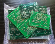
Very nice boards - congratulations!
Have fun,
Toni
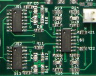
Thanks. I made a couple of silly mistakes with the silkscreen but I don't think it's the end of the world. Just disappointing. I hope the board tests ok!
Attachments
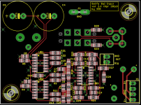
Fellow DIYer astx (Toni) has been kind enough to conduct some testing of the board.
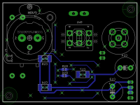
The first finding was that my supply bypassing with 0.1uF from rail to rail was insufficient. I have amended the board to accommodate 0.1uF from each rail to signal ground. I've left provision for caps from rail to rail as well. I should have made the board more flexible in the first place.
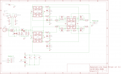
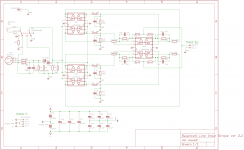
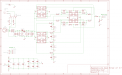
The second issue identified is an interesting one. I have attached the schematic for the board that went to fabrication below (first pic). While testing single-ended input, Toni found that it was necessary to ground the path to pins 4 and 5 of U$1 and U$2 (I will from now on call this the "pin 3 path") on the right side of C3. The board, as fabricated, has provision to ground the pin 3 path by jumpering R28 but only on the left side of C3. Toni measured -110dB A-weighted referred to 4V RMS if the grounding occurred on the left side of C3 (by jumpering R28) but -130dB (his measurement limit) if he grounded the pin 3 path on the right side of C3. Note that a grounding of the pin 3 path is tantamount to connecting the single-ended "cold" to pins 4 and 5 - the connection is via the ground plane.
It's interesting to step back a little at this point and reflect on Bruno Putzey's two articles: The G Word, or How to Get Your Audio Off the Ground and section 4.5 of Dealing With Legacy Pin 1 Problems. In the former he stresses that a balanced input need not have symmetrical pin 2 and 3 signals - one can be static or constant, even at 0V. In the second article he deals with connecting single-ended sources into a balanced input.
Bruno's articles would suggest the better way to connect single-ended cold (single-ended hot is connected to pin 2 as outlined in his article) is to pin 3 and potentially with an RC filter to the chassis. Also a trace could used rather than the signal ground plane.
I find it puzzling that the two scenarios measure rather differently. The + single-ended signal is going through the full pin 2 path. Toni also found he needed to add connect single-ended cold not just to xlr pin 3 but also to signal ground via a 10R resistor. Yet I believe Bruno intends that the input be floating.
I'd be interested in anyone's thoughts on all this. Toni please correct or add to my summary of the testing.
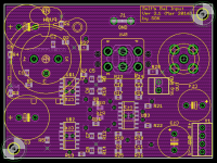
I have amended the board to correct the bypassing, fix the orientation of the toggle switch and shift the break in the pin 3 path to the right side of C3. The other thing Toni suggested was adding provision for a voltage divider at the output for more flexibility - either merely to add a minimum load or to add attenuation. Images attached.
The first finding was that my supply bypassing with 0.1uF from rail to rail was insufficient. I have amended the board to accommodate 0.1uF from each rail to signal ground. I've left provision for caps from rail to rail as well. I should have made the board more flexible in the first place.
The second issue identified is an interesting one. I have attached the schematic for the board that went to fabrication below (first pic). While testing single-ended input, Toni found that it was necessary to ground the path to pins 4 and 5 of U$1 and U$2 (I will from now on call this the "pin 3 path") on the right side of C3. The board, as fabricated, has provision to ground the pin 3 path by jumpering R28 but only on the left side of C3. Toni measured -110dB A-weighted referred to 4V RMS if the grounding occurred on the left side of C3 (by jumpering R28) but -130dB (his measurement limit) if he grounded the pin 3 path on the right side of C3. Note that a grounding of the pin 3 path is tantamount to connecting the single-ended "cold" to pins 4 and 5 - the connection is via the ground plane.
It's interesting to step back a little at this point and reflect on Bruno Putzey's two articles: The G Word, or How to Get Your Audio Off the Ground and section 4.5 of Dealing With Legacy Pin 1 Problems. In the former he stresses that a balanced input need not have symmetrical pin 2 and 3 signals - one can be static or constant, even at 0V. In the second article he deals with connecting single-ended sources into a balanced input.
Bruno's articles would suggest the better way to connect single-ended cold (single-ended hot is connected to pin 2 as outlined in his article) is to pin 3 and potentially with an RC filter to the chassis. Also a trace could used rather than the signal ground plane.
Essentially a differential input is a floating input. Nothing more, nothing less. The only reason why one should consider including an RC combination is to keep the signal within the common mode range of the input circuit (remember that the source may be floating) and to keep RFI that’s been picked up by the RCA cable out of the box.
I find it puzzling that the two scenarios measure rather differently. The + single-ended signal is going through the full pin 2 path. Toni also found he needed to add connect single-ended cold not just to xlr pin 3 but also to signal ground via a 10R resistor. Yet I believe Bruno intends that the input be floating.
I'd be interested in anyone's thoughts on all this. Toni please correct or add to my summary of the testing.
I have amended the board to correct the bypassing, fix the orientation of the toggle switch and shift the break in the pin 3 path to the right side of C3. The other thing Toni suggested was adding provision for a voltage divider at the output for more flexibility - either merely to add a minimum load or to add attenuation. Images attached.
Attachments
Note: my measurement equipment and/or setup may give not so good noise figures if RCA cold is connected on left side of C3...
The signal flow was:
BR, Toni
The signal flow was:
- SE output of VP-7723D to
- Steve's balanced2se converter bal. input
- Steve's balanced2se converter SE output to
- bal. inputs of (same) VP-7723D
BR, Toni
Sounds like C3 is managing to introduce 20 dB of A-weighted noise all by itself. That's surprising.Toni measured -110dB A-weighted referred to 4V RMS if the grounding occurred on the left side of C3 (by jumpering R28) but -130dB (his measurement limit) if he grounded the pin 3 path on the right side of C3.
Also sounds like you expect to measure -110dB on the unmodified unit when you insert a shorting plug into the XLR socket. Then with the shorting plug in place, you expect to measure -130dB when you short the two terminals of C3 together. (Left terminal is already ground thanks to the shorting plug).
The pos. inputs of the lme49740 are ultra sensitive. I've added 22p parallel to R5 and R6 and the distortion and noise figure betters significant. Maybe a loop on pcb due to the 2 ground layers and/or lme49740 needs some caps directly at inputs to supress oscillation and avoid rf noise?
BR, Toni
BR, Toni
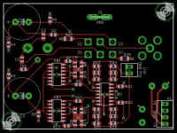
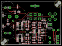
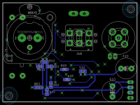
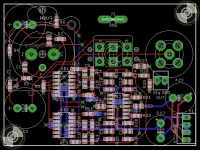
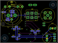
Revised version. Better decoupling, better routing, larger resistors etc. Layer 2 used for routing also. Only one ground plane. Will be sent to ASTX Labs for testing shortly!
Attachments
Last edited:
Revised version. Better decoupling, better routing, larger resistors etc. Layer 2 used for routing also. Only one ground plane. Will be sent to ASTX Labs for testing shortly!
Very nice - looking really good. Can't wait for testing ...
")
Yes they are. Sorry, I keep forgetting to remove the + from the silk or rather I am too lazy to create a custom part in Eagle just for this. Self recommends 35V. The board will take 470u - the bigger the better. I am using these. My BoM attached.
You don't want to raise the value of the input resistor - doing so will increase noise.
You don't want to raise the value of the input resistor - doing so will increase noise.
Attachments
Last edited:
the input resistors from signal flow to return do not increase the noise. The Receiver sees the Source Impedance and that sets the effective resistance noise.Yes they are. Sorry, I keep forgetting to remove the + from the silk or rather I am too lazy to create a custom part in Eagle just for this. Self recommends 35V. The board will take 470u - the bigger the better. I am using these. My BoM attached.
You don't want to raise the value of the input resistor - doing so will increase noise.
Only when the interconnect is disconnected will the Receiver see the resistors. In this disconnected condition the noise will be worse.
The factor for noise is sqrt(Rnew/Rold) and changing from 47k//100k to 100k//100k gives +1.94dB more noise in the disconnected condition.
I would accept this and change to a 1u8F polypropylene capacitor.
If this were at the Power Amplifier input I do use 100k and 1uF for F-3dB=1.6Hz
How many Builders use Zin=100k and complain that that resistor value causes excessive noise?
Last edited:
Apologies, for some reason I thought you meant increasing the two 100R resistors R1 and R2, even though when I read your text again it is clear you meant the 47k.
Out of interest, which would you suggest and how big is it? If the electrolytic is large enough distortion is extremely low. Hence selecting 470uF. (Fig 2.21 Self's SSAD 2nd ed.)
Out of interest, which would you suggest and how big is it? If the electrolytic is large enough distortion is extremely low. Hence selecting 470uF. (Fig 2.21 Self's SSAD 2nd ed.)
Last edited:
In the spirit of keeping common-mode input impedance high, consider a T-type configuration for input resistors (where the 47k ones are now) - e.g. 10k + 10k with midpoint going to signal ground via 100k. (That's 20k differential and 110k common-mode.) Likewise for capacitors, maybe 470p+470p and 47p.
I'm not sure why one would be particularly worried about noise contribution of these resistors. Do you listen with the input open? In use they will be shunted by source Z anyway.
470µ bipolar sounds pretty massive, I am sure most people would consider 100µs generous in this spot. I don't necessarily think that "the more the merrier" - what with leakage current?
Keep in mind that balanced connections tend to be run 6 to 12 dB hotter than unbalanced ones in practice, and lower-than-unity gain may be called for on the receiving side. Consult schematics / specs of sending side of in doubt.
Many balanced impedance sources are specified to drive 600ohms loading.
That is probably why 470uF is shown. Jensen show 220uF for driving 600ohms.
If one knows that 2k, or 5k, or 10k, is a minimum worst case loading on the Source, then a much smaller coupling capacitor can be adopted.
That is probably why 470uF is shown. Jensen show 220uF for driving 600ohms.
If one knows that 2k, or 5k, or 10k, is a minimum worst case loading on the Source, then a much smaller coupling capacitor can be adopted.
From D.self: 470µF shows best THD figures down to 20Hz.
At load 1k, 10Vrms:
BR, Toni
At load 1k, 10Vrms:
- 220µF shows 5ppm THD decreasing to 2 ppm to 50Hz - 20kHz.
- 470µF only 2ppm - flat to 20kHz.
BR, Toni
The point is that the load isn't anywhere close to 1k here, as should be plainly obvious from the schematics given. As suggested, we're talking 10k, or 47k as shown above (plus ~120 ohms (give or take) of source impedance). Even when taking potential capacitance mismatch into account that might reduce low-frequency CMRR (bonus points for 5-10% tolerance parts or hand-matching), 100µ seems plenty big enough.
- Home
- Amplifiers
- Solid State
- Self's "5532 Low Noise Unity Gain Balanced Input Stage"