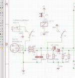
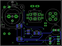
.................... Or rather, having it on a device having its signal ground tied to PE is. Inputs like that rely on classic "GND think". ...................
The input socket pin2 is shown connected to ground, twice.....................Signal GND is not tied to PE. The only connection to PE via XLR pin 1 is the initial RF filter, the idea being to not pollute signal ground with any RF noise. (The GND of the supply caps returns to the supply. All other connections are to an isolated Signal Ground.)...............
It's the classic mistake made by nearly everyone that thinks all "grounds" are the same. And then draws the schematic like that.
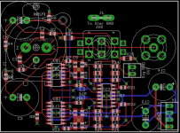
Pin2 should connect to R2, C3, R5 AND C7
R3 is HBRR/HBRL in D.Joffe's paper. This is ONLY required where one has two (or more) channels inside the same chassis. Monoblocks do not need HBRR/HBRL
The Output needs a voltage reference to the Input, HBRR/HBRL (R3), or a wire/trace link, provides this voltage reference.
There are no chassis/ground/Earth connections to pin2.
Pin 2 is Signal Return and it route needs to be close coupled to the Signal Flow route to minimise LOOP AREA.
Do not take pin2's connection on a journey around the amplifier looking for a ground.
Last edited:
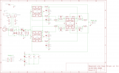
I'm not using the 5532. The idea is to implement the design and work tested by Self. His work on this topic started with the 5532, then graduated to the newer LM4562 (and he went on to better it with the AD797 which I have avoided).
Yes, I had to create the part in Eagle from scratch and I could have drawn a bunch of separate triangles... Or placed the triangles within a rectangle as did the data sheet when depicting its pin configuration. In the end, I went for the latter as less chance of error and easier-to-follow routing. I don't find it hard to flick between the two presentations.
As to the THAT products, as noted above that is where I started having read the material at the Elliot Sounds site. I was steered away from such implementation (BTW I note that Bruno rejected them also as the distortion wasn't good enough for him) towards implementing one of Self's designs. I'm trying to apply what I have learnt from reading his text. There's lots of ways to skin a cat.
The Bruno article sgrossklass provided the link for is a great read and, like most things Bruno, compelling. But I am not looking to reinvent the front end of Toni's amp typology. This project was just a basic building block to be able to build his amp with balanced inputs.
pictorial 'schematics'
Yes, I had to create the part in Eagle from scratch and I could have drawn a bunch of separate triangles... Or placed the triangles within a rectangle as did the data sheet when depicting its pin configuration. In the end, I went for the latter as less chance of error and easier-to-follow routing. I don't find it hard to flick between the two presentations.
As to the THAT products, as noted above that is where I started having read the material at the Elliot Sounds site. I was steered away from such implementation (BTW I note that Bruno rejected them also as the distortion wasn't good enough for him) towards implementing one of Self's designs. I'm trying to apply what I have learnt from reading his text. There's lots of ways to skin a cat.
The Bruno article sgrossklass provided the link for is a great read and, like most things Bruno, compelling. But I am not looking to reinvent the front end of Toni's amp typology. This project was just a basic building block to be able to build his amp with balanced inputs.
The input socket pin2 is shown connected to ground, twice.
It's the classic mistake made by nearly everyone that thinks all "grounds" are the same. And then draws the schematic like that.
Pin2 should connect to R2,
Pin 2 ONLY connects to R2. I don't follow you. Note the question posed in post 1.
Last edited:
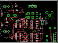
At the moment, it hasn't changed since post 45. I reproduce the relevant bit below (so stratus46 doesn't have to look at my pictorial schematic ") ). Your point is the essence of the question I had when I started this thread. Yes, as currently configured I have tied the initial RF filters R1/C2 and R2/C1 to the chassis along with XLR pin 1 (the XLR component has a GND pin which is tied to connector's shell and on to the chassis when assembled in place). From post 1:
). Your point is the essence of the question I had when I started this thread. Yes, as currently configured I have tied the initial RF filters R1/C2 and R2/C1 to the chassis along with XLR pin 1 (the XLR component has a GND pin which is tied to connector's shell and on to the chassis when assembled in place). From post 1:
As you can see, I was asking about how to manage ground structures (a whole battle Bruno would suggest is somewhat pointless and best avoided via sticking to fully differential signalling). I take it you are saying don't do this; rather, tie C1 and C2 to the board's GND plane. Correct?
BTW the question of where to tie ground of the supply reservoir caps is part of the same issue. (These aren't shown in the snip below, sorry.) I had them tied to 'signal ground' on this board while Toni suggested tying them back to the supply's 'dirty' ground.
Of course, all these grounds are eventually tied together via a star ground. I take it that the idea behind this is that supply GND currents should circulate 'locally' before being connected to other ground planes. The star ground eventually connects to chassis and PE. And so C1 and C2 eventually connect to PE just like XLR pin 1. The question is via which route is best...
BTW I note that in the article by Bruno linked to above, his equivalent of R1/C2 R2/C1 (I really should reorder the names of these) are tied to XLR pin 1.
). Your point is the essence of the question I had when I started this thread. Yes, as currently configured I have tied the initial RF filters R1/C2 and R2/C1 to the chassis along with XLR pin 1 (the XLR component has a GND pin which is tied to connector's shell and on to the chassis when assembled in place). From post 1:It seemed sensible to me (a novice) to ground, at least, the HF filters R1/C2 and R2/C1 via Pin 1 / Pin GND on the XLR connector, i.e. directly to chassis, rather than letting any RF enter the circuit (signal) ground.
As you can see, I was asking about how to manage ground structures (a whole battle Bruno would suggest is somewhat pointless and best avoided via sticking to fully differential signalling). I take it you are saying don't do this; rather, tie C1 and C2 to the board's GND plane. Correct?
BTW the question of where to tie ground of the supply reservoir caps is part of the same issue. (These aren't shown in the snip below, sorry.) I had them tied to 'signal ground' on this board while Toni suggested tying them back to the supply's 'dirty' ground.
Of course, all these grounds are eventually tied together via a star ground. I take it that the idea behind this is that supply GND currents should circulate 'locally' before being connected to other ground planes. The star ground eventually connects to chassis and PE. And so C1 and C2 eventually connect to PE just like XLR pin 1. The question is via which route is best...
BTW I note that in the article by Bruno linked to above, his equivalent of R1/C2 R2/C1 (I really should reorder the names of these) are tied to XLR pin 1.
Attachments
Last edited:
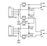
What is the purpose of showing the post56 sch.
That is the post that has the pin2 connected to ground twice.
Why did you post that?
That is the post that has the pin2 connected to ground twice.
Why did you post that?
am I making a stupid mistake with all this? (Schematic excerpt attached.)
What is the purpose of showing the post56 sch.
That is the post that has the pin2 connected to ground twice.
Why did you post that?
Ah sorry. I replied before you had finished editing your post. The schematic in post 56 is Toni's IPS/VAS. Pin 2 there is signal ground from the output of the input board. Apologies, but I thought it was obvious that I provided an excerpt from Toni's schematic to aid readers thinking about the question I posed about signal current and estimating total current needs of this input board.
Your questions and advice in relation to his schematic are best addressed to Toni.
... and need to know the input impedance of the IPS/VAS that this line receiver is driving. Toni, do you have the latter for your SA2014? Is it basically just the parallel resistance 47k || 8.2k or am I making a stupid mistake with all this? (Schematic excerpt attached.)
Can I take it that you are fine with the connections shown in post 65, the excerpt from my schematic to which this thread relates?
Last edited:
so what do we do with this question?am I making a stupid mistake with all this? (Schematic excerpt attached.)
No. Pin2 is Signal Return. It is NOT ground anything !Pin 2 there is signal ground from the output of the input board.
Ok. My sloppy choice of terminology. Hand smacked. And it connects to pin 2 of my board's output socket which is, in turn connected to the board's plane(s) on the two middle layers. The four differential amplifiers use these as a reference also. Please correct my terminology.
EDIT: frankly thinking in terms of 'signal' and 'signal return' is much less intuitive for me than thinking of it as differential signalling. I think of this input board as converting a differential signal carried by XLR pins 2 and 3 to a (differential) signal at output connector "Signal Out - Right" where pin 1 there is a voltage with reference to pin 2. || OOH, I SHOULD USE CONSISTENT PINS TO AVOID LATER ERROR.|| This reference point for Signal Out needs to be carried forward with the signal to the amp module. In a perfect world the reference point would remain the same throughout. Bruno's point that there's no need to mix at all the Signal Reference Point (my term) and 'ground' resonates well with me. But I've jumped onto the 'classical' playing field he abhors and I'm trying to implement best practice within it.
Well my question was how to estimate the current need of the board under max signal conditions.
EDIT: frankly thinking in terms of 'signal' and 'signal return' is much less intuitive for me than thinking of it as differential signalling. I think of this input board as converting a differential signal carried by XLR pins 2 and 3 to a (differential) signal at output connector "Signal Out - Right" where pin 1 there is a voltage with reference to pin 2. || OOH, I SHOULD USE CONSISTENT PINS TO AVOID LATER ERROR.|| This reference point for Signal Out needs to be carried forward with the signal to the amp module. In a perfect world the reference point would remain the same throughout. Bruno's point that there's no need to mix at all the Signal Reference Point (my term) and 'ground' resonates well with me. But I've jumped onto the 'classical' playing field he abhors and I'm trying to implement best practice within it.
so what do we do with this question?
Well my question was how to estimate the current need of the board under max signal conditions.
Last edited:
Use the LTSPICE "UniversalOpamp2" as an easily measured, approximate model of an opamp. The datasheet tells you the DC bias current drawn from the power supplies; to that you will add the signal-dependent power supply current measured on your UniversalOpamp2 model.
Start with opamp #1. Have your UOA2 drive opamp1's load resistor at maximum possible signal amplitude. Enough amplitude to ensure that the downstream thingaboo (power amplifier?) is driven into clipping. Set the opamp's load resistor to its lowest possible value. Don't forget to include all sources of load capacitance, since power is consumed when you charge and discharge capacitors. Measure the supply current when the input is a 22 kilohertz sine wave. Average over an integer number of cycles.
Now do the same with opamp #2. You could build a whole new .asc file or you could just add another UOA2 to your first file, with its own unique load resistor and load capacitor.
Repeat with opamps #3 thru #2N.
Although the above approach may seem clumsy at first glance, it does completely sidestep the scary monster of calculation which flummoxes and plagues many non-EEs. Instead of calculating signal-dependent power, you merely model and measure it. Less frightening.
Finally: consider asking yourself the question, why not feed a perfect 22 kilohertz SQUARE WAVE through a 180kHz lowpass filter (single pole passive RC lowpass) and use that waveform as the input to my models-of-opamps? Wouldn't that be the most difficult possible test for power consumption? Don't I want to know an worst-case upper bound on signal-dependent power consumption?
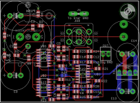
I'm back at this circuit. I changed the layout so that the board fits on the same plane as the connectors (which in turn support the board) and inserted a toggle switch for input selection. I'm just waiting for the PCB footprint of my RCA connector before sending the boards to fab. For now I have added a footprint which would allow soldering solid 1.5mm copper wire connections to a Cardas GRFA-S RCA connector.
At the moment I have the switch shorting the RCA Hot to signal ground when balanced input is selected. I'm not sure if this is better than leaving it open-circuited. My gut tells me the latter would be preferable as there is then no chance of noise coupling into the GND plane from the RCA connection...
At the moment I have the switch shorting the RCA Hot to signal ground when balanced input is selected. I'm not sure if this is better than leaving it open-circuited. My gut tells me the latter would be preferable as there is then no chance of noise coupling into the GND plane from the RCA connection...
Attachments

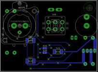
At the moment I have the switch shorting the RCA Hot to signal ground when balanced input is selected. I'm not sure if this is better than leaving it open-circuited.
Short it to ground through a 1206 size, 50 ohm resistor. This lets you change your mind later. You can remove the resistor (changing its value to Infinity ohms), you can solder a wire across its terminals (changing its value to Zero ohms), or you can desolder it and replace with any other resistance value you wish, according to the fashion of the times.
Your PCB layout has plenty of room, you could use a socketed thru hole resistor instead, and put on a resistor change-a-thon festival.
Hopefully this is now ready to go to the board house for fabrication (finally). I made a few changes:
1. I changed the switch routing in relation to XLR pin 3. When the input is switched to single-ended, the input from Pin 3 is now either open circuited or grounded, depending on whether R28 is populated. So it conforms to what I had done with the single-ended input if balanced input was selected. It does, however, make for a longer trace from R1/C1 to the switch and back down to C3 (rather than a more direct connection).
If you guys tell me this is inadvisable I will reverse it. In the first instance I was not planning to populate R27/28 i.e. leaving the unselected input open circuited rather than connected to signal ground.
2. Changed the packages of the 0805 SMD resistors and caps to wave soldering which gives a bit more pad length to make hand soldering that much easier.
3. Finalised the package for the RCA connector to take a Cardas GRFA PS (drawing). This and the XLR connector should support the board nicely.
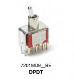
4. I keep going back and forth regarding solder pads for the frame of the C&K switch versus just holes. (Image attached.) Flicking this switch is the only time the user can place strain on the board's mounting on the XLR and RCA connectors. Initially I was thinking the frame could be removed from the switch altogether but that would seem to require a special tool that can grip the key hole. This draft has solder pads/holes for the frame legs but perhaps I will change them back to just holes as any strain would be mostly lateral.
1. I changed the switch routing in relation to XLR pin 3. When the input is switched to single-ended, the input from Pin 3 is now either open circuited or grounded, depending on whether R28 is populated. So it conforms to what I had done with the single-ended input if balanced input was selected. It does, however, make for a longer trace from R1/C1 to the switch and back down to C3 (rather than a more direct connection).
If you guys tell me this is inadvisable I will reverse it. In the first instance I was not planning to populate R27/28 i.e. leaving the unselected input open circuited rather than connected to signal ground.
2. Changed the packages of the 0805 SMD resistors and caps to wave soldering which gives a bit more pad length to make hand soldering that much easier.
3. Finalised the package for the RCA connector to take a Cardas GRFA PS (drawing). This and the XLR connector should support the board nicely.
4. I keep going back and forth regarding solder pads for the frame of the C&K switch versus just holes. (Image attached.) Flicking this switch is the only time the user can place strain on the board's mounting on the XLR and RCA connectors. Initially I was thinking the frame could be removed from the switch altogether but that would seem to require a special tool that can grip the key hole. This draft has solder pads/holes for the frame legs but perhaps I will change them back to just holes as any strain would be mostly lateral.
Attachments
Last edited:
I would keep pin3 connected, not switchable to open.
Pin2 and Pin3 are the normal balanced impedance input.
When an unbalanced input is required you can still use Pin2 and Pin3. Provided the switch to convert to unbalanced does not open circuit pin3.
Pin2 is always signal Hot.
Pin3 can be signal cold (balanced impedance) or signal return/ground (unbalanced)
If you want RCA in parallel to pins 2 & 3, they don't need to be switched, just left empty. But you do need to ensure that adding the unswitched RCA does not unbalance the impedance, particularly the stray capacitances.
Even the switched RCA must not unbalance the impedances when in balanced impedance mode. Here is where a very small signal relay using the NO pins as the balanced connection minimises the stray capacitance and pay attention to balancing the differences of stray capacitances
Last edited:
Hi Andrew.
Originally all inputs were connected to the signal flow. Jan's suggestion in post 9 was to ground the unused input (the XLR pin 3 path) when single-ended is selected. I added to this the complementary grounding of the single-ended hot input if balanced was selected.
It then occurred to me that rather than grounding unused inputs, which would feed any rubbish coming in from an unused connection into the signal ground plane, it would be better to open circuit them. Mark noted that both options could be worked into the board by adding two resistors. These could be 0R, direct grounding of the particular unused input, grounding via resistance X, or not populated for open-circuiting of unused inputs.
Your suggestion would take me back towards the original position...
Note the switch is needed/can't be omitted.
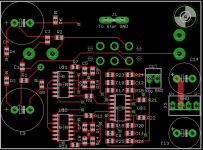
I will add some mounting holes top right and bottom left, but the idea is that it doesn't need them. Rather the board is supported by the XLR and RCA connectors.
Thats OK. The mounting holes are for the only case, where one doesn't use the same XLR and RCA connectors ...
BR, Toni
- Home
- Amplifiers
- Solid State
- Self's "5532 Low Noise Unity Gain Balanced Input Stage"