I wonder if a mini high voltage version of this might be a good supply for a front end in a dual supply application.
I'm also working on a bulk supply with CM boosted rails that track the main rails to stay a specific voltage over them.
I'm also working on a bulk supply with CM boosted rails that track the main rails to stay a specific voltage over them.
Sounds perfect for a lateral output amp.
Yes, jwilhelm is correct. I was beginning to wonder what you were seeing there Paulo ") .
.
Anyhow, I could still step down from a maximum 40mmø main capacitor to 35mmø and reduce the output capacitors ones from 25mmø to 16mmø and shrink the whole thing some. I wanted the layout to accommodate the wide range of sizes so folks could source components more easily. That was also the motivation to making the diff amp BJT based as well.
.Anyhow, I could still step down from a maximum 40mmø main capacitor to 35mmø and reduce the output capacitors ones from 25mmø to 16mmø and shrink the whole thing some. I wanted the layout to accommodate the wide range of sizes so folks could source components more easily. That was also the motivation to making the diff amp BJT based as well.
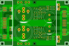
If you are going to need a double-sided board, then I think you should make full use of the copper on both sides. If you rearrange the output terminals to have all + on one side and - on the other, then you could duplicate the ground track between the reservoir capacitors and output on both sides of the board, halving its resistance and inductance. Yes, that does mean you will have a short length of untwisted wires next to the terminals, but you effectively already have that on the PCB itself.
jkuetemann,
I checked and double-checked the MOSFET datasheets on Fairchild's website, and I am pretty sure your PCB layout in post#26, applies the rippling raw input voltage to the MOSFET source, and takes the filtered not-so-ripply output voltage from the MOSFET drain. I believe this is an error. A severe error.
I believe what you intended to build, is a source follower with ENORMOUS amounts of capacitance on the gate, thereby producing an incredibly tiny impedance "Zgate" at the gate, which is further reduced at the output (source) as Zout_source_follower = (Zgate / gm).
But (if I'm correct!) you have regrettably reversed source and drain, so at high currents when the body diode turns on, the output will be shorted to the input through a diode, and you won't get much ripple attenuation at all.
Please have a look and see what you think.
Whoops, never mind, I failed to see that the +Supply pass device is a Pchannel and the -Supply device is an Nchannel. Thus they are Common Source Amplifiers (just like the series pass transistors in Low Dropout retulators) and are hooked up correctly.
My bad.
Sorry for the distraction!
My bad.
Sorry for the distraction!
It seemed to me like very big pcb but compared to PMI's board it is in fact only about an inch longer. So it probably is as compact as possible. Will I be able to use parts that I obtained for PMI's board, parts from MrEvil's original schematic?
I'd have to look to see what the pin-out for the specified MOSFETs is, but I didn't really have the intent to follow the original that closely. There should be no reason the diff amp can't still be done utilizing the small MOSFETs. After some playing about, both in simulation and on the bench, I may return a little of the complexity I stripped out by adding back CCSs for the diff amp tails. This will make the circuit insensitive to the average bulk supply voltage value. I still plan to leave the mirrors off though, the single resistor works well and too simple to ignore.
I intended this one to utilize inexpensive and easily sourced BJTs (been working with the KSA992F and KSC1845F). I also created a pass MOSFET footprint that allows TO-220 / TO-3P / TO-247 / TO-264 devices, so choosing a different output device is easy too.
The size shouldn't be too serious a hurdle, I have made other boards this size and found no issue with fitment when constructing with it in mind. Mine is about 6mm wider and 30mm longer then the PMI version, but I can accommodate a wider range of capacitors. All of my main traces are also much beefier and this takes up space too. Everything is a trade-off. My goal is wide parts acceptance. Retro-fitting into a prior build of course may be another story.
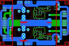
I re-oriented a couple things and re-routed a few traces. With a few added pads for jumpers / links this could be done as a single sided home etch board, though that isn't my current priority since I have fallen in love with the quality and ease of use with board house production. Current snapshot attached. I still have a few things to add, this is just a look at the current state. I tried to make better use of the top copper as well.
Attachments
A little testing...
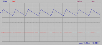
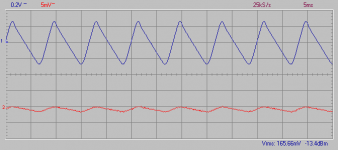
A little testing with a prototype this evening. Output ripple was measured with a DC current being drawn at two levels, 250mA and 2.5A.
My test set-up is built on a scavenged old junk components. The transformer gives me a lightly loaded 27V rail. I was using a 25A bridge module and 25mF of bulk capacitance. The CM is based on a BJT differential amplifier and an LED biased current source for the tail current. The pass device is a P-channel MOSFET configured 'common source'. Basically as previously published only with a CCS for the tail current. I placed a small 1000uF output capacitor instead of the larger 4700uF specified.
First image is for a 250mA draw. Input ripple is about 68mV peak to peak and there is no discernible output ripple. The 'drop-out' was set to 2V. This was to emulate a quiescent class AB or 'optimal bias' B amplifier.
The second shows a 2.5A draw. Input ripple was about 540mV peak to peak and output ripple was about 2mV peak to peak. The supply sagged to an average DC level of only 20V under this test. The 'drop-out' measured at 1.7V at this current draw.
I think the results are encouraging. PCB artwork is nearing completion, just housekeeping at this point. I think this might just be worth getting some in for a proper build and testing. Thoughts?
Attachments
Since the circuit is a cascade of two stages, each stage having gain>1, there may be some lingering concerns about stability margins. Perhaps you could use a 555 oscillator chip and a NChannel MOSFET to switch the load current back and forth between 0.25A and 2.50A at 1 kHz, and look at the transient response? Maybe there's overshoot and ringing?
Is the "Drop-out" the voltage drop of the circuit from rectifier to output? If so 1.7 volts under load is much better than I expected.
I'm sure I mis-used the term 'drop-out'. in my usage the 'drop-out' voltage is the voltage difference between the input and output, so effectively what is across the MOSFET. It could be run with less drop-out, down to about 1V with the caveat that it becomes more likely that the circuit will pass ripple to the output under load. I chose 2V to give plenty of margin.
Bear in mind that I'm abusing this with DC current draw and with real use playing music there will likely be no issue running the output closer to the input. If a little ripple poked through on a loud, bass-laden passage would you even be aware? I doubt it.
This is looking like a promising supply for my VSSA amp. I was expecting a larger voltage drop. I've already purchased a transformer for it and was concerned the voltage drop would be too great. Do you think it might possibly improve by starting with a higher voltage transformer and dropping 5 volts?
- Home
- Amplifiers
- Power Supplies
- Simplified MrEvil / PMI Capacitance Multiplier