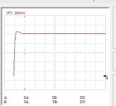
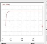
For future test purposes solder 100 Ohm 5 Watt wire wound resistors across the fuse holders and remove the fuses. When you switch on keep your fingers on the switch and moisten the index finger on your other hand and bring this close to the body of the resistor for the positive voltage supply but not touching if you feel heat rising switch off if not measure the voltage drop across the resistor. The bias transistor should be set for minimum output standing current.. I have no interest in building this amplifier or doing simulations despite the fan base this design has attracted as I have reservations over the design which raise some questions that you may be able to answer.With my DMM on diode test or continuity mode, whatever you like to call it
the 2SA1943 behaves the following:
B to E = OL
E to B = 0.54
B to C = OL
C to B = 0.55
E to C = OL
C to E = OL
A fresh 2SA1943 gives
B to E = OL
E to B = 0.69
B to C = OL
C to B = 0.6
E to C = OL
C to E = OL
The 2SC5200:
B to E = 0.03
E to B = 0.01
B to C = 0.45
C to B = OL
E to C = OL
C to E = 0.045
A fresh 2SC5200 gives
B to E = 0.539
E to B = OL
B to C = 0.53
C to B = OL
E to C = OL
C to E = OL
So it appears to me that I have a fried 2SC5200 but the 2SA1943 has survived.
All of the 1943 and the 5200 chips I have let through a silver of light when held back to back up to a light, just a hair.
The brand new ones have what I would call a dull surface on the back.
All the transistors were purchased from Mouser back in December 2019.
View attachment 1216119
View attachment 1216118
The first one concerns setting the output stage standing current which in your case is higher than what Rod Elliot recommended.at 75 m.a. are you able to set the working channel to Rod's recommendation and does that remain constant after reaching equilibrium in terms of heat sink temperature?
Looking at the issue raised by ostripper looking at the cfp arrangement with R12 set at 220R that will cause Q5 to bias Q7 on. When it comes to reducing conduction the base charges in Q7 i.e. electrons need to be partially discharged by holes via R12 reverse connection to holes present in the positive power supply. This is less likely to work than would be the case if R12 value was 100R. There should be as equal traffic flow of charges as possible in either direction. This is lopsided in my view and should have been considered by Rod Elliott
If R12 was set at 100R and an addition 100R was to be fitted between Q5 emitter and R13 that objective might be achieved since Q5 will operate driving Q7 in split phase. It is highly doubtful that would be so inthe opposite circuit half due to c6
.
The IO wiring is not the tidiest. The inputs go around the PSU however the left output does go over the top, this was an older photo where it went underneath.Is there a schematic for the power supply, and the other little board? Is there an overall interconnection wiring diagram that includes where all grounds are physically connected? Also, in the picture, can you confirm which is electrically the left and right channel?
In addition, it looks like there is some randomly routed I/O wiring. Just poking some of that stuff around might show some symptoms. Hard to say exactly from looking at the pic.
This was due to laziness as I had some pre terminated speaker cable and I didn't want to make a fresh one.
The amp boards are orientated from the point of view of the listener. Left is right and right is left from the perspective of the photo.
Here is the PSU.
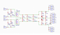
The extra little board is an ESP P33 speaker protection. Currently the output of the amp boards is not connected, it is simply providing AC detection for the output relays.
This is how the wiring goes:
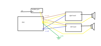
With the speaker protection properly implemented, there would be a signal wire from the output of each amp board to the input of the speaker prot but I have omited this as it is currently not implemented.
Rod recommends 25mA-100mA so I aimed for the middle of the range.For future test purposes solder 100 Ohm 5 Watt wire wound resistors across the fuse holders and remove the fuses. When you switch on keep your fingers on the switch and moisten the index finger on your other hand and bring this close to the body of the resistor for the positive voltage supply but not touching if you feel heat rising switch off if not measure the voltage drop across the resistor. The bias transistor should be set for minimum output standing current.. I have no interest in building this amplifier or doing simulations despite the fan base this design has attracted as I have reservations over the design which raise some questions that you may be able to answer.
The first one concerns setting the output stage standing current which in your case is higher than what Rod Elliot recommended.at 75 m.a. are you able to set the working channel to Rod's recommendation and does that remain constant after reaching equilibrium in terms of heat sink temperature?
Looking at the issue raised by ostripper looking at the cfp arrangement with R12 set at 220R that will cause Q5 to bias Q7 on. When it comes to reducing conduction the base charges in Q7 i.e. electrons need to be partially discharged by holes via R12 reverse connection to holes present in the positive power supply. This is less likely to work than would be the case if R12 value was 100R. There should be as equal traffic flow of charges as possible in either direction. This is lopsided in my view and should have been considered by Rod Elliott
If R12 was set at 100R and an addition 100R was to be fitted between Q5 emitter and R13 that objective might be achieved since Q5 will operate driving Q7 in split phase. It is highly doubtful that would be so inthe opposite circuit half due to c6
.
I had no issues with setting bias on either channel.
I slowly increased the bias current over a period of an hour. After setting it at 50mV (75mA) it was steady at 50mV +/- 0.5mV for half an hour of observation before I called it a night.
How about the input wiring, and its grounding?This is how the wiring goes:
You ever seen this app note: https://www.mikrocontroller.net/att..._User_s_Guide_to_Decoupling_and_Grounding.pdf
The gnd wire from the rca sockets goes directly to the amp boards.
The input gnd goes straight to the power gnd on the amp boards.
Each of the input commons should go to their respective amp board common, while being twisted with the input hot lead.
Or use shielded cables connected in the same way.
H
HAYK
Attachments
Last edited by a moderator:
I didn't explain it very well but that is exactly how it is wired.Each of the input commons should go to their respective amp board common, while being twisted with the input hot lead.
Or use shielded cables connected in the same way.
I have used a twisted pair from a cat5 cable for the input wiring. Colored being hot and the striped being the common.
G'day guys,
This evening I had the time remove and measure Q4 and Q5.
Q4 has failed, Q5 measures fine.
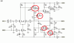
So here is what has blown.
Now the question I have to ask myself is do I
A) assume I got unlucky and reinstall fresh transistors to replace those that have failed and hope everything works properly this time.
B) Do A and also reroute the IO wiring to be more optimal guessing that this might have had an influence on the poor results.
C) Go about trying to 'fix' the design.
I am inclined towards option B, if I run into more issues then perhaps I need to look at option C or move onto another design.
This evening I had the time remove and measure Q4 and Q5.
Q4 has failed, Q5 measures fine.

So here is what has blown.
Now the question I have to ask myself is do I
A) assume I got unlucky and reinstall fresh transistors to replace those that have failed and hope everything works properly this time.
B) Do A and also reroute the IO wiring to be more optimal guessing that this might have had an influence on the poor results.
C) Go about trying to 'fix' the design.
I am inclined towards option B, if I run into more issues then perhaps I need to look at option C or move onto another design.
I will disagree.
Melted back plate can't be an indication of counterfeit transistor but a genuine one!
Counterfeit transistor destroy fast before temperature raised and melt the plate.
Melted back plate is an indication that this worked hard in high temperature before oscillations destroy the body.
BTW i have a fully working P3A years now .
Pcb isn't the original by Eliot but a clone by Alexmm
I used BD130-149 in driver position and MJL21193-94 in the output
Amplifier is rock stable even without R.L filter in the Output.
Last edited:
I could sim the thing.
But have spent endless time fixing and stabilizing CFP designs here many times.
The semi conductor choices were fine.
Problem is this amplifier isn't friendly to modern high gain high FT semi conductors.
And I wouldn't expect it to do much more than oscillate.
The value for R6 alone in rods schematic is likely not the right value and would cause massive amounts
of DC offset. And the output section would just ring ring ring.
Amongst other band aids usually seen to make a CFP design stable.
Combined with bootstrap gain stage, DC offset and all together unstable design
in the first place.
Needs a current mirror to somewhat help the horrid DC offset or R6 would have to be adjustable.
Needs Degen in differential stage. Removal of ancient CFP band aids.
Remove poop strap current source etc etc.
One channel didnt destroy itself instantly. But shows heavy oscillation likewise. ( expected )
So it wasnt just one bad channel.
Not trying be negative. Its sad to see nice transistors tortured by a misleading design.
I would quickly abandon it to save money and sanity.
Could fix it but the board doesn't have the additional components needed.
Even if fixed, would always remain marginally stable and why CFP has been
abandoned by many. Just more grateful that it didnt destroy any speakers.
Which would be the outcome from all the DC on the output when the devices fail again
Last edited:
... The value for R6 alone ...massive amounts of DC offset...
I measured around 65mV on my six P3A, which, by the way, run without problems now for more than ten years.
I tuned R6 and R7 a bit and went down to about 15mV DC offset. Unfortunately not well documented by me, I decreased R6 and increased R7 slightly.
For the two amps feeding the tweeters I replaced the whole input V-I stage with a SoA current mirror, which decreased also distortion noticeable.
btw, the 1kHz sine plots shown in the first post show substantial oscillations also for the "well performing" amp. Tedious to count, but I guess the frequency is around 70 to 100kHz. The "bad" trace shows additional frequency noise of much higher frequencIes, but this trash is not continuous, but starts around 90% after the maxima/minima. What does this tell us?
I do not agree.I will disagree.
Melted back plate can't be an indication of counterfeit transistor but a genuine one!
Please find me another one with the same faults .
Tells us exactly what I described. And exactly as you described.
R6 needs to be fine tuned and expect high DC offset in your case 65mV
You fixed the issue as I described using a mirror.
Doesnt need a mirror but with DC offset even around 3mV to 15mV
expect the negative rail to still ring like crazy with high Ft high gain transistors.
Also expect the usual bandaid and add a cap to negative rail driver transistor.
Which usually causes more ringing with high Ft transistors
and highly dependent value based on the exact transistors used.
Bootstrap second gain stage is fun yes. CFP with high Ft outputs.
Nope ring ring ring. Just like the scope is showing.
Needs usual 100n across thermal track transistor.
That is if DC offset was actually below 5mV and the negative rail not ringing.
But it will do that regardless because the DC offset without adjusting R6 will
always be there.
And when its gone, the bootstrap wont work, Vas will ring, negative rail will ring.
No degen in differential, Driver bandaid not removed.
Use ancient transistors shown in rods schematic, use band aids shown
and cross your fingers and expect the usual high DC offset.
These simple designs work no problem without mirrors and boot straps.
Easy fix, remove the CFP output stage and use slow Darlington's.
Otherwise using high Ft transistors and rods simple circuit = nope
Apply another huge bandaid over the feedback loop. Darlingtons no problem.
CFP = rings more. Needs degen, DC offset less than 3mV, no bootstrap, bandaids removed.
pretty much impossible. Velleman K8060 same amp, pnp differential instead.
doesnt oscillate and high DC offset like any other simple design.
Has Darlington's instead and compensation that actually works.
Bootstrap second gain stage and same high 2nd order distortion.
The only magical thing that people hear when their P3A isnt busy oscillating.
People scream murder and troll K8060 threads, when a P3A is same thing.
Just prone to oscillate
= abandoned
Agree yes, scope shows high frequency oscillation. As expected.
Go with the usual advice, make the input RF filter capacitor so large.
It makes dirt slow outputs stop ringing. Another typical band aid
Again wont work with High Ft transistors. And not the way to stabilize a amplifier
regardless
Last edited:
Okay. The point is has been made pretty convincingly that this is not really a tested and working design, especially if using modern substitute transistors.
Should we assume the OP was looking a simple, low-cost design which is reliable? Say, as opposed to a more complex and costly design which is better sounding?
Should we assume the OP was looking a simple, low-cost design which is reliable? Say, as opposed to a more complex and costly design which is better sounding?
Nothing wrong at all with a simple design.
Overall simple design is a good decision.
And high quality semi conductors from trusted source purchased.
Did everything right really, and assembled a working amplifier.
Isn't his fault the design is a oscillator.
Overall simple design is a good decision.
And high quality semi conductors from trusted source purchased.
Did everything right really, and assembled a working amplifier.
Isn't his fault the design is a oscillator.
Build a simple amp that does not have the "High Ft" issue. (below).
Green LED like the P3A , I've used junkbox 2N5401/5551 , MPSA92/42 ... any
old e-waste 2SC/A outputs (and new NJW high Ft ones).
ANYTHING works ! Junkbox special...
Oh , "low cost design that does not sound good?" .... no issue with that here.
This is the design that "hooked me" back in 2008 !
OS
Green LED like the P3A , I've used junkbox 2N5401/5551 , MPSA92/42 ... any
old e-waste 2SC/A outputs (and new NJW high Ft ones).
ANYTHING works ! Junkbox special...
Oh , "low cost design that does not sound good?" .... no issue with that here.
This is the design that "hooked me" back in 2008 !
OS
Attachments
- Home
- Amplifiers
- Solid State
- Stability testing my new Rod Elliot P3A

