I guess I don't know how to run this type of file because after I run it I only see 0V everywhere. I'm working on another amp right now. When I get finished with it I will measure this regulator and mark up a schematic so maybe you can help me find the issues.
Thanks, Terry
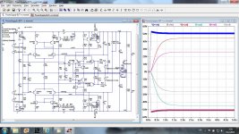
Terry I did say how to get the waveforms after the simulation finished. Just put the cursor on the place where you want to see the voltage or current graphs and click the right mouse baton. With that way you can get all the voltages and the currents in form of graphs or waveforms. In this simulation you cant read that just by positioning the cursor on the schematic. It is quite simple, jus run all three .asc files one by one and, as with the amp simulation, click the mouse on the same way when you want to see, per example, output voltage, or output load current.
BR Damir
Hi Damir,
Thanks for trying to help me. Trying to read the graph is not specific enough for me to discover the problem. I have another amp on the bench right now. When I get that done I will take some measurements and mark up a schematic and we'll try to go from there.
Thanks again, Terry
Thanks for trying to help me. Trying to read the graph is not specific enough for me to discover the problem. I have another amp on the bench right now. When I get that done I will take some measurements and mark up a schematic and we'll try to go from there.
Thanks again, Terry
Hi Damir,
Thanks for trying to help me. Trying to read the graph is not specific enough for me to discover the problem. I have another amp on the bench right now. When I get that done I will take some measurements and mark up a schematic and we'll try to go from there.
Thanks again, Terry
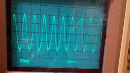
Hi terry,
Maybe this will help you, and it should look like this. Just run the simulation and some waveforms - traces should be there. You can add or remove traces as much as you like.
BR Damir
Attachments
OK I see it now. How do you make the background white? Mine is black.
Go to Tools, choose Waveform, than Color Scheme, than Selected Item and choose Background and select the color you prefer. In that way you can choose the color for any Selected Item.
Hi Guys,
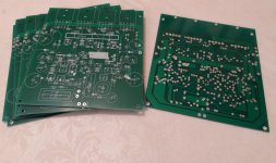
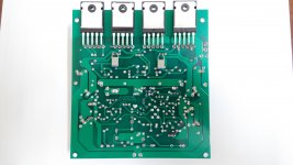
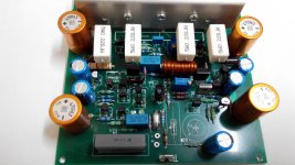
I know some of you expressed an interest in building this amp. Now that I have got mine working properly, I would like to share the other three pair of boards that I have. If you are interested in buying a pair or two, please PM me. I have some extra outputs I can let go reasonably too if you need.
Blessings, Terry
Hi Damir,
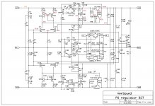
No, I set it aside so I could finish my A33 and Valery's tube hybrid. Now that those are working I will get back to the regulator. I'll post a schematic with voltage readings tomorrow. Is it better for you to see voltage readings or voltage across resistors? I suppose I could do both.
Blessings, Terry
Hi Damir,
No, I set it aside so I could finish my A33 and Valery's tube hybrid. Now that those are working I will get back to the regulator. I'll post a schematic with voltage readings tomorrow. Is it better for you to see voltage readings or voltage across resistors? I suppose I could do both.
Blessings, Terry
Hi Terry,
Voltage reading is enough, but don't forget to disable both sides protection before you switch on.
BR Damir
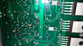
Sorry man, I tried all day. I can't get it to work. I have 0.00 VBE on both pass transistors. I bypasses R13 and R113 and still no good. I have a fluctuating +30V on the positive output and 1.3V on the negative output. I have checked and double checked each transistors. They are all correct and all read good with a diode test. There is something wrong but I can't find it. If I put a load on it the negative output goes to zero. I'll post some voltages in the morning and we'll go from there.
Hi Terry,
It is simpler to troubleshoot the PS regulator if you test first positive side only. Connect just the plus and the ground from the power supply to the PS regulator, disable that side protection and it should work, I don't see why not. If you've got correct output voltage (5 to 6V less that input voltage and don't forget some load) then you can proceed with both sides.
BR Damir
You are so right. I just checked again and the 2n5xxx have reversed layout to the silk. These layout errors have taken all the fun out of this project.
Sorry Terry, all small transistors are TO-92 with the outline of BC5xx types. This is DIY and if you check the pin out you can insert correctly those with different outline. I used different transistors from those in schematic in my boards as the types are not critical, just the Vceo, actually with your voltages you can use BC556/546 for TO-92 transistors.
My apology for your inconvenient.
BR Damir
How high a rail voltage was this designed to operate at? I will spin the 2N5xxx transistors. I actually thought I had checked the pinouts when at first it didn't work. I guess I was mistaken. I will fix it in the morning and report back. This is the last thing on my work bench. Going to need a new design to try building after this.
How high a rail voltage was this designed to operate at? I will spin the 2N5xxx transistors. I actually thought I had checked the pinouts when at first it didn't work. I guess I was mistaken. I will fix it in the morning and report back. This is the last thing on my work bench. Going to need a new design to try building after this.
That depends of the used transistors for Q2, Q3, Q6, Q7, Q8, Q9 and corresponding other side transistors. If you use BC546/556 than it could be used up to 60V. With 2N5551/5401 much higher, but then some more simulation is needed if the voltage is over 60V.
If you are up to challenge look this amp http://www.diyaudio.com/forums/solid-state/216780-tt-amp-200w-8ohm-701w-2ohm-3.html#post3119028
Layout was never made for this one.
Hi Damir,
Thank you for this wonderful amplifier.
I finally managed to assemble two channels and had a first listen yesterday.
All I can say is that's a very good sounding amplifier that I can highly recommend.
It's very quiet, smooth, balanced, with firm bass and delicate highs.
In my build at least I had to deal with a couple of problems that I would like to mention:
1. I had a parasitic oscillation of aprox. 100Mhz which I tracked down to the input cascode pair.
Putting a small cap from Q3, Q4 base to ground solved this (I tried various values (3.3uF, 100nf, 1.5nF all of them working fine) and finally installed a small 4.7nF MKT in that position)
2. I installed a BAV21 diode from Q12 collector to Q15 base which slightly improved clipping behavior.
Now I only notice a very slight sticking in the negative side.
I also would like to mention that I deviated from the suggested list of parts
and used a pair of 2SK170-BL as input fets, KSA992 and KSC1845 instead of 2SA970 and 2SC2240 and BD139 instead of 2SC3503 for Q1(I would appreciate your opinion about the changes Damir, are they O.K. by you?).
Future builders should also in addition to suggestions of posts #453 and #463 install a wire link in R15 position and shouldn't forget C19 and C24 which I put in the underside of the PCB.
A big thanks also to Terry who was kind enough to order and send me two pcb's that made this build possible.
Best regards,
George
P.S. In my final build I installed C3, C4 and D11 as offset was too high for my liking without them.
Attachments
- Status
- This old topic is closed. If you want to reopen this topic, contact a moderator using the "Report Post" button.
- Home
- Amplifiers
- Solid State
- ThermalTrak+TMC amp