A couple of observations/comments:
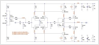
I attached a version with a few tweaks that seems to perform well and is in the same spirt as your original design. The biggest change is running the JFETs at a set lower current rather than running at Idss. I also have the VAS running a little hotter.
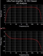
- The design appears to be very stable into capacitive loads without the need for an inductor. I see no hints of square wave ringing into 100n up to 2u.
- It clips well. I was expecting sharper corners due to the high feedback ratio, but this is not the case.
- DC Offset sensitivity seems OK. If you alter ambient temp, device temp, and/or the rails, the DC offset fluctuates around 20mV.
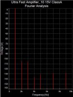
- FFT plots show predominately lower order distortion up to around 10W. It is not low distortion, but does have a monotonically descending spectrum, which I suspect will sound good.
I attached a version with a few tweaks that seems to perform well and is in the same spirt as your original design. The biggest change is running the JFETs at a set lower current rather than running at Idss. I also have the VAS running a little hotter.
- I added P1 to allow the current through the JFET to be set rather than letting the JFETS run ad Idss. In your original, I believe the performance could vary considerably based on the Idss of the devices used.
- I altered the manner in which the DC offset is adjusted.
- I added R12 & R13 to allow the output bias to be measured and adjusted via P2.
- I lowered the values of the feedback network to lower noise
- I lowered the value of the input resistor to lower noise
- Loop gain shows 60db / 60 degrees of margin with a 1MHz ULGF.
Attachments
Last edited:

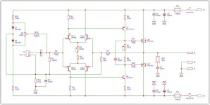
A single pair Lateral MOSFETS design shouldn't need source resistors. I was thinking the 0.1R resistors might be better placed before the caps to create a bit of RC power supply filtering. So that they can serve two purposes.
To my knowledge this is a simulation only design at this point.
Regarding DC offset trimming... there's many ways this could be done. Lineup had a different approach in his design. I'm sure there are other ways to do it.
To my knowledge this is a simulation only design at this point.
Regarding DC offset trimming... there's many ways this could be done. Lineup had a different approach in his design. I'm sure there are other ways to do it.
Reminds me of the first amp on this page https://2adiy.ovh/sche.html, by monsieur Plantefeve.
More like the one in the middle of the page if it wasn't for the cascode'sReminds me of the first amp on this page https://2adiy.ovh/sche.html, by monsieur Plantefeve.
I like the offset trimming here, I think maybe it would be nicer with a single low value pot with the wiper on the feedback line?
I am not sure exactly where this will wind up on the post, but here are some of my observations:
Overall a very nice design, and I am working on a variation - a Transnova idea from Jim Strickland - in which I replaced R8 with a TLVH431 and resistor pair combo, such that if the pot fails with the wiper open, which in my experience is the most common case, the bias will collapse to about 1.2V total, and the mosfets will be "safe". Another advantage of this approach is the bias voltage to the mosfets is largely independent of the collector current flowing through the VAS stage, eliminating the pot in the upper VAS transistor's emitter.
Also as a further aside, in my simulation experiments so far, the Hegglun models do more accurately simulate the transfer characteristics of the actual mosfet as opposed to the Exicon models; I set up simple sims to step thru gate and drain voltages to reproduce the characteristic curves. The Exicon models have a distinct discontinuity at the boundary of the triode to saturated region. The bummer is that Multisim does not support the VDMOS model; LTSPice does.
I believe that I would test the simulation with some RLC models of speakers, I believe that Rod Elliott has described some. Use a complex load.
That's really informative design guides. I wonder what if the input still uses BJT pairs but with FET buffered.A couple of observations/comments:
- The design appears to be very stable into capacitive loads without the need for an inductor. I see no hints of square wave ringing into 100n up to 2u.
- It clips well. I was expecting sharper corners due to the high feedback ratio, but this is not the case.
- DC Offset sensitivity seems OK. If you alter ambient temp, device temp, and/or the rails, the DC offset fluctuates around 20mV.
- FFT plots show predominately lower order distortion up to around 10W. It is not low distortion, but does have a monotonically descending spectrum, which I suspect will sound good.
I attached a version with a few tweaks that seems to perform well and is in the same spirt as your original design. The biggest change is running the JFETs at a set lower current rather than running at Idss. I also have the VAS running a little hotter.
- I added P1 to allow the current through the JFET to be set rather than letting the JFETS run ad Idss. In your original, I believe the performance could vary considerably based on the Idss of the devices used.
- I altered the manner in which the DC offset is adjusted.
- I added R12 & R13 to allow the output bias to be measured and adjusted via P2.
- I lowered the values of the feedback network to lower noise
- I lowered the value of the input resistor to lower noise
- Loop gain shows 60db / 60 degrees of margin with a 1MHz ULGF.
For me, it seems to improve the input stage transconductance and achieves a more linear action. Also the idle current will be less dependent on the FET Idss.
Attachments
Sure it seems good enough, and i like the symmetrical design. But to build a real version it is not so diy friendly because of the exotic jfets. So I thought it is worth exploring alternatives for the input devices. You could use BJT's there, or matched J113/J176 jfets that are 20 times cheaper and easy to get.
I'd suggest keeping it simple. Cascodes, mirrors, etc can be added to make it "better", but I think the appeal of this design is its simplicity.
I'd also suggest sticking with the LSK489/LSJ689. If you switch to J113/J176, the devices are individually cheaper, but you'll likely need to order 100 or each to match them. These are around $18 for 100 at Digikey which is twice the price of one LSK489/LSJ689. And you still need to go through the exercise of matching, and then selling the other matches you may find to recoup some expense. Doesn't seem worth it to me.
You can get most of the parts from DigiKey with the exception of the LSJ689s and the Laterals. DigiKey offers the LSK489 in grades but suppliers for the LSJ689 do not. The LSJ689 can be found at NAC Semi and the Exicon Lateral can be bought direct from Profusion.
I tested the design with LSK489 in B grade and then varied LSJ689 between A, B and C grades. Performance didn't seem to vary that much. But this is a big reason I suggest a trimmer and running the IPS at a specific current and not Idss. Otherwise, you will need to match the LSJ689 and LSK489 which will get tricky and expensive.
Lineup specs the design with ±20V rails and 500mA of bias. This should work in a 2U chassis with running too hot. This should provide around 15W into 8Ω.
However, with the parts designated, it should be safe up to ±35V rails which should provide around 50W into 8Ω. To run in the same 2U chassis, the bias would probably need to drop to 200mA to 300mA. At this level, there is still some safety margin for the LSJ689 which is spec'd at 50V Vgs.
However, with the parts designated, it should be safe up to ±35V rails which should provide around 50W into 8Ω. To run in the same 2U chassis, the bias would probably need to drop to 200mA to 300mA. At this level, there is still some safety margin for the LSJ689 which is spec'd at 50V Vgs.
Just coming back to the idea of using more common parts I thought I would test to see how it would work.

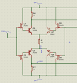
I'v added Q3 and Q4 as to help drive the FETS as they are 3x higher input capacitance as the original design, this also allows for less current and more gain in the VAS.
C4/C2 added to help prevent possibility of oscillations but may not be necessary.
I'v added Q3 and Q4 as to help drive the FETS as they are 3x higher input capacitance as the original design, this also allows for less current and more gain in the VAS.
C4/C2 added to help prevent possibility of oscillations but may not be necessary.
Here is a low power version, but it works in full Class A.
Output is like 8 Watt with a 2x12VAC transformer.
Bandwidth: almost 4 MHz
Dist at 1 Watt: THD 0.00077%
Heatsink: 2x24 Watt for stereo

Output is like 8 Watt with a 2x12VAC transformer.
Bandwidth: almost 4 MHz
Dist at 1 Watt: THD 0.00077%
Heatsink: 2x24 Watt for stereo
Attachments
To buy for example LSJ689 dual monolitic JFET:
https://store.nacsemi.com/Products/Detail?part=LSJ689-TO-71&stock=LIS000000001308&Mfr=LINEAR SYSTEMS&auth=y&utm_campaign=listing&utm_source=findchips&utm_medium=aggregator&utm_content=textlink&instock=Y
or here:
https://lukaseparts.se/butik/diy-ko...l-ultra-low-noise-capacitance-jfet-transistor
https://store.nacsemi.com/Products/Detail?part=LSJ689-TO-71&stock=LIS000000001308&Mfr=LINEAR SYSTEMS&auth=y&utm_campaign=listing&utm_source=findchips&utm_medium=aggregator&utm_content=textlink&instock=Y
or here:
https://lukaseparts.se/butik/diy-ko...l-ultra-low-noise-capacitance-jfet-transistor
- Home
- Amplifiers
- Solid State
- Ultra Amplifier with JFET input and Lateral MOSFET out