Wonky resistors are a possibility.
I curently have the board removed from the amplifier and can certainly access the resistors more easily for testing.
My actual reason for removing the power amp board is to better see the traces. Some solder pads had lifted and some trace portions may have been obliterated creating the need for jumpers. I wish the make sure that certain component pins like those of Q406 are going where they are supposed to go. I thought they were because the amp was working but with this recent removal and replacement of parts, I am not so sure anymore.
The component placement diagram is not of high enough resolution to depict the foil traces in their entirety so I need to use the schematic as a guide. And have a clear head.
There are always errands to run, appontments to keep and my dog needs to be driven several times per day for exercise periods lasting an hour or so, Unless I am dragged somewhere tomorrow, I should have a couple of hours to concentrate on this board.
I had more idle time before I retired, moved away from a big city and got a dog.
@Mooly ,i still think it's worth checking the surrounding resistors. I know the obvious burned ones were replaced, but there could be the odd failure without any visual sign don't you think?
Yes of course, but I am assuming the resistors in the output stage have been tested as OK. We have to stick with the theory and work from that and this 0.7 volts biasing the drivers can possibly be turning them and the output stage on. There are only two resistors (R315 and R328) apart from the 330 ohm and 0.47 ohm in that area and given 'perfect' transistors with zero leakage even if both those were open there should still be zero bias current.
Without a scope we are limited in diagnostics but it might be worth putting a meter on AC volts (a low range) and see if there is any AC voltage across resistor R324 in the Zobel network. Its clutching at straws because of limitations using a DVM for that but if it showed a voltage we might have clue that some oscillation was occurring.
Lets wait and see what happens ")
This might help the op in understanding how it works and how all the numbers fit into place. This shows just the output stage lifted from the previous simulation. The bias generator goes from zero volts to 4 volts over 10 seconds. The chart shows bias voltage and the current in one of the 0.47 ohm resistors.
The voltage is on the left scale and current on the right. The bias voltage (the voltage between the two 330 ohm resistors) has to reach almost 2.8 volts before any current flows in the output stage. The 2.8 volts is needed to overcome all the base/emitter junctions of the stage.
Green trace is the voltage between the 330 ohm resistors. Left scale.
Red trace is the current in one of the upper 0.47 ohm resistors. All four 0.47 ohm have the same current flowing. Right scale.
It is worth checking that the 2.7k and 1k are good and not open circuit.

In simulation if we add a tiny leakage current to the pre driver (the bottom PNP transistor here marked Q7) by adding a 2 meg between collector and emitter and if we also open circuit the 2.7k we do get a small current flow in the outputs. This is why those two resistors need checking.
The current is now not zero:

This is the circuit in its reduced form:

This might help the op in understanding how it works and how all the numbers fit into place. This shows just the output stage lifted from the previous simulation. The bias generator goes from zero volts to 4 volts over 10 seconds. The chart shows bias voltage and the current in one of the 0.47 ohm resistors.
The voltage is on the left scale and current on the right. The bias voltage (the voltage between the two 330 ohm resistors) has to reach almost 2.8 volts before any current flows in the output stage. The 2.8 volts is needed to overcome all the base/emitter junctions of the stage.
Green trace is the voltage between the 330 ohm resistors. Left scale.
Red trace is the current in one of the upper 0.47 ohm resistors. All four 0.47 ohm have the same current flowing. Right scale.
It is worth checking that the 2.7k and 1k are good and not open circuit.
In simulation if we add a tiny leakage current to the pre driver (the bottom PNP transistor here marked Q7) by adding a 2 meg between collector and emitter and if we also open circuit the 2.7k we do get a small current flow in the outputs. This is why those two resistors need checking.
The current is now not zero:
This is the circuit in its reduced form:
I certainly hope that represetation was quick and painless. I have only just now seen it and due to my limited comprehension. it will take much pondering to absorb.
The last time I dipped a toe in transistor theory was a grade 10 high school electroncs class in 1968. It was tacked on as fill once they were done trying to make us understand vacuum tubes.
As I mentined in my last post, for ease of access and to better view the trace side, the board is removed from the amplifier chassis. I was concerned about the damage already done to solder pads with particular concern about Q406.
I removed (again) Q406 and cleaned away as much solder as I could from the trace side so as to make sure it's pins connected with what they were supposed to connect with. Fortunately, they were. I had to compensate for two missing solder pads and am pretty confident I can re-install it sucessfully.
As for the resistors, I measured all of the 1/4 and 1/2 watt resistors on the right channel. I counted 22.
Except for 3 or them, all resistors measured within spec. The ones that did not are:
R421: supposed to be 68K but measured 53K
R425: supposed to be 4.7 ohms but measured 0.3 ohms
R420: supposed to be 270K but measured 53K
I'm pretty sure he said he only replaced The burned ones and didn't test any others
Yes, that was correct. But I checked all right channel resistors this evening and posted the findings.
VeryI certainly hope that represetation was quick and painless.
This kind of thing is a very real possibility. Typically a pad can crack where it connects to the rest of the print and these can be very hard to spot visually.I was concerned about the damage already done to solder pads with particular concern about Q406.
It is very rare for a resistor to go low in value and even then it is mostly resistors of a specific material (metal oxide) that can do this. R425 is across the series output coil and so all you are reading is the coil itself... its fineR421: supposed to be 68K but measured 53K
R425: supposed to be 4.7 ohms but measured 0.3 ohms
R420: supposed to be 270K but measured 53K
High value resistors should always be checked out of circuit to prevent interaction with other components but at this point I wouldn't worry over doing that. Something much more fundamental is going on with this fault.
The takeaway point of the simplified simulation is to show that 0.7 volts DC between the two 330 ohm resistors can not give rise to any bias current flow. The DC part is important. High frequency oscillation can not be read on a meter.
There is one other possibility that is worth checking. If there is a short on the speaker output feed somewhere then that will show as a high bias current as the offset voltage of the amp tries to drive current into the short. That scenario would cause a current to flow in either the upper or lower pair of 0.47 ohm resistors but not both. Which pair would depend on the offset polarity.
Definitely worth checking for a short as measured across the speaker terminals.
To satisfy my curiosity I lifted a leg of those two resistors that read low and yes, when out of circuit they displayed their correct value.
I then hooked up the board and proceeded with raising variac voltage while watching the DBT. And yet again, the DBT began glowing at 50/60 volts. With power off, I used DMM at the speaker terminals to check for shorts. Left channel had no short, display read OL.
When moving to right channel, the DMM's audible continuity alert chirped for a second and the numeric display was erratic. Readings quickly rose and fell willy nilly ranging from OL to seral hundred ohms. After a time, the display settled down and began a steady climb topping out at 900 ohms after a minute or so.
I am at the pont of considering this amp a lost cause.
Several years ago, I experienced a damaged board in a Teac open reel recorder. The more I worked at it, the more damage i created. As a last resort, I looked at ebay listings for a Teac board with the same part number and actually found one. When I transferred the new components I installed on the old, damaged board to the new undamaged board, the recorder was able to operate.
It is unlikely but possible I suppose that a Sony board would pop up but I don't think Sony made anywhere near the numbers of these TA-1150 amplifiers as Teac did of those recorders so I won't be holding my breath.
I would like to get this Sony amp out my sight at least for a while.
According to the schematic it should read around 940R if not less - are you sure you had the speaker terminals connected when measuring?.With power off, I used DMM at the speaker terminals to check for shorts. Left channel had no short, display read OL.
I am at the pont of considering this amp a lost cause.
Lets try one totally 'out there' idea before giving up on this.
Remove this circuit breaker on the speaker output on the relevant channel and see if the bulb still lights as before (or not).
I discovered that I reacted to another error I made.
When I reconnected the left channel speaker wire to the board, I slid it onto the wrong pin. I had it on the bias test point pin, not it's correct pin. The two are quite nearby each other.
With that oversight rectified, the DBT is dark when the variac is at full power.
Now that the wires are on their appropriate pins, there are 900 ohms on each channel.
DBT in place and variac at full, I next checked left and right bias. Both channels read 4.5 volts and are not adjustable.
EDIT: Without letting the amp idle for a time,, there was 30mV offset on left channel and 4.5 volts offset on right channel.
When I reconnected the left channel speaker wire to the board, I slid it onto the wrong pin. I had it on the bias test point pin, not it's correct pin. The two are quite nearby each other.
With that oversight rectified, the DBT is dark when the variac is at full power.
According to the schematic it should read around 940R if not less - are you sure you had the speaker terminals connected when measuring?.
Now that the wires are on their appropriate pins, there are 900 ohms on each channel.
DBT in place and variac at full, I next checked left and right bias. Both channels read 4.5 volts and are not adjustable.
EDIT: Without letting the amp idle for a time,, there was 30mV offset on left channel and 4.5 volts offset on right channel.
Last edited:
OK, that's good that you have found thatWhen I reconnected the left channel speaker wire to the board, I slid it onto the wrong pin. I had it on the bias test point pin, not it's correct pin. The two are quite nearby each other.
Well that's something.With that oversight rectified, the DBT is dark when the variac is at full power.
4.5 volts??? Do you mean millivolts.... or... ?DBT in place and variac at full, I next checked left and right bias. Both channels read 4.5 volts and are not adjustable.
I thought one channel was basically OK or has that channel also had its transistors changed to match the other one?
4.5 volts??? Do you mean millivolts.... or... ?
I thought one channel was basically OK or has that channel also had its transistors changed to match the other one?
It is 4.5 volts not millivolts.
The right channel was receiving all the attention and the left channel seemed "normal". However, yes, yesterday I did replace the left channels transistors to match those of the right channel.
My reason was that since I had the board out of the amplifier to assess the traces, pads and reconstruct if needed, that I may as well do both channels at the same time, Since that involved removing Q405 and Q406 as well as Q305 and Q306 I thought that installing BD140 and BD139 at Q305/306 now instead of re-installing what was there then doing another re and re later would cause less harm to the foil.
So at this time, Q305 and Q306 are BD140/BD139, same as Q405 and Q406. If it was a masochistic thing to do, I apologize but I replaced the left channel's output transistors also so that they match those of the right. This was to minimize disconnecting and reconnecting the board to the amplifier.
The metal sleeves at the ends or the wires are basically a socket that slip onto the board's connector pins. Those socket connectors are flimsy and need crimping each time I reconnected them. Without crimping with pliers they fit loosley. I was worried that with continued crimping they would break/fail.
With that in mind, I did look at some suppliers websites for new replacments connectors but didn't see any that looked compatible.
Therefore I cut to chase by installing new transistors now instead of later so as to maipulate the board less frequently.
It's late, I'm tired and I hope this makes some sense.
It's late, I'm tired and I hope this makes some sense.
Lets look at key points. Read or at least try the last bit first...
This shows a definite problem. The fact the bulb is also not lit suggests something is open circuit or the print is open somewhere or there is an undetected error in the work done.DBT in place and variac at full, I next checked left and right bias. Both channels read 4.5 volts and are not adjustable.
The bias measurement is simply looking at the voltage across one of the 0.47 ohm resistors. Its the same method in 99.9% of designs. So 4.5 volts across 0.47 ohm would be a current of 4.5/0.47 which is over 9.5 amps. That's not possible for lots of reasons
The bulb can't pass that for one thing, even just the mains transformer alone couldn't deliver that even if you wanted it to... so something fundamental is wrong.I would begin by looking at the voltage across each of the four 0.47 ohm resistors. If one or more show any substantial voltage like this 4.5 volts then the resistor has to be open.
If this 4.5 volts is not present across any 0.47 ohm and yet you measure this voltage when connecting the meter in the way described in the manual then there must still be an undiagnosed error in the wiring.
Other possibilities are that there might still be some further 'error' in the way its all been put back together.
One other thought. Just check there is continuity from here to here (arrowed in red) which is the + speaker terminal to the junction of all the 0.47 ohm resistors. Also make sure that CB1 arrowed in blue reads short circuit. If this was open and you had a DC offset of 4.5 volts then it would also make the bias reading also appear as 4.5 volts. This seems the most likely scenario at this point.
One other thought. Just check there is continuity from here to here (arrowed in red) which is the + speaker terminal to the junction of all the 0.47 ohm resistors. Also make sure that CB1 arrowed in blue reads short circuit. If this was open and you had a DC offset of 4.5 volts then it would also make the bias reading also appear as 4.5 volts. This seems the most likely scenario at this point.
I looked for continuity between +speaker posts and the legs of all 0.47 ohm resistor legs and found none.
I tested across the pins of both circuit breakers and there was continuity - neither was OL.
There was some voltage measured across the right channel 0.47 ohm resistors.
R319 1.8mV
R317 100mV
R318 3.2mV
R316 3.4mV
All 4 resistors on the left channels measured 0.0mV.
Yes, there is still 4.5 volts present at both left and right bias adjustment points.
There is no reason to believe that I did not commit some wiring errors. The most likely spots I think would be the areas around Q406 and Q306. Those had the most "butchery" done to their solder pads and traces. I did my best, I thought, to create jumper bridges but could have easily screwed up.
That was my reason for recently uninstalling Q406 and Q306 and clean up as best I could. To expose as much as possible of their trace area to see what went where but I could have made the wrong best guess.
It's a pity the component placement diagram in the service manual was not more legible. It would have helped immensely as a map.
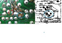
What the trace side looks like presently, after adding jumper bridges is not much better. Unfortunately, I have not been able to navigate Microsoft Paint so have been unable to highlite the pins of Q406 and Q306.
Lets work with this. Look at the circuit. There should be continuity (provided the speaker speaker switch is set correctly).I looked for continuity between +speaker posts and the legs of all 0.47 ohm resistor legs and found none.
The bridging looks fine but just make sure there are no shorts. This looks like it might be touching the print next to it but I know 2D pictures are often not easy to interpret accurately and it may be fine.
Lets work with this. Look at the circuit. There should be continuity (provided the speaker speaker switch is set correctly).
The speaker switch is switched to speaker A which are the top row of this group of terminals. Blue is right speaker + and green is left speaker +. There is continuity between those speaker posts and each group of four 0.47 ohm resistors.
However, continuity is with the opposite resistor group. Left speaker + has continuity with the right channel resistors and right speaker + has continuity with the left channel resistors.
This came about just after acquiring this amplifier. There were two faults I corrected right away. One was replacing the pilot or power on lamp and the other was the balance control. When I got the amp, the balance control was reversed. So I swapped sides with these two wires, red and white that go to the speaker switch.
Once done, the balance control operated correctly. I assumed that whoever worked on the amp prior to 2019 when I bought it, got them reversed and I was just correcting their mistake. I never gave it another thought until now.
Now I am not sure how the balance control got reversed. It seemed I was rectifying someboey's oversight. But, since left channel power amp is now driving right speaker and right channel power amp is now driving right speaker, then correcting it needed to be done elsewhere.
It would be nice of the power amp's left channel drove the left speaker and right channel drove the right speaker but I'm thinking this has no bearing on the issue(s) at hand, But I could be totally wrong about that.
The bridging looks fine but just make sure there are no shorts. This looks like it might be touching the print next to it but I know 2D pictures are often not easy to interpret accurately and it may be fine.
I am amazed that that photo made sense to you. And yes, that "blob" does look like it touching the trace. But it's is not. As you mentioned, it's camera angle. The prominence is the trimmed end of the wire I used to create that bridge
If I'm right those 2 solder points should be joined to the right of where mooly has circled
Is what's circled in blue the two solder points you refer to?
- Home
- Amplifiers
- Solid State
- Adjusting an old bias pot did some damage and I am unsure how to proceed