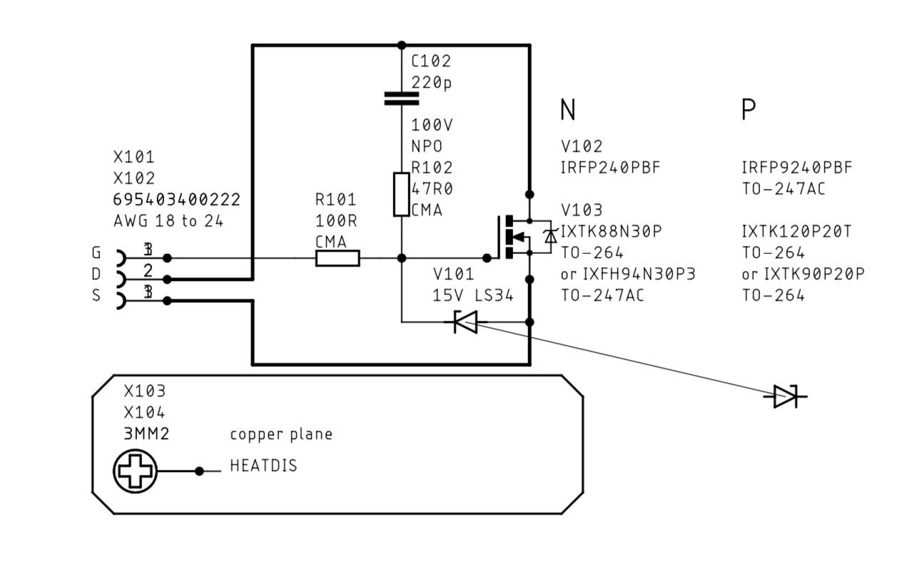
Snubber schematics. IXYs can be used (like on ABBB) but FQAs are more cost effective for this level of thermal dissipation. N.B., the orientation of the Zener depends on N or P channel.
Yes - particularly for the 4R version - it seems sensible to use:
* FQA40N25, and
* FQA36P15
... for V141 & V142, as per your 8R 'As Built' schematic.
However, I am a tad confoosed by your Snubber diagram & text:
1. V101 (between the Source & the Gate of V141 & V142) is a 15v Zener, right?
2. V103 (between the Source & Drain of V141 & V142) is another Zener. What voltage is this?
3. So what is V102?
Or is this a mistake - and it should really be V141?
Thank you, Andy. You are doing all of us in this thread a huge favor.
I have to admit there's more than a bit of self-interest in what I'm doing!

Andy
Andy,
The protection system between gate and source of mosfets is normally a single Zener of 15V configured to fire at the point where the gate potential reaches 15V wrt the potential on the source. On a nmos, this is +15V and on a pmos it is -15V.
However, a trick to minimise assembly issues there is a non-polar technique to use a double zener, with conjoined cathodes, strung across gate to source from anode to anode. On the nmos, anode is at gate, the top zener will fire at 0.6V (reverse zener) but the next, bottom zener will not fire until it has 15V across it, meaning a total pd across anode to anode is then 15.6V. These dual zeners are available in SOD23, very tiny, and you only need to connect gate to source anode to anode. The single conjoined point is not connected to anything, and this configuration works with both mosfets types. It avoids the polarity/wiring issues.
Thank you very much for setting up the 4R BOM with cataloguing. Much appreciated!
Hugh
I then V102 and V103 refer to the two possible MOSFETs that can be mounted there. N channel and P channel. The Zener you see near V103 is the internal Zener built in, inside the MOSFET.
The back to back conjoined SOT23 Zener would have reduced the orientation issues - it’s probably smaller than the MELF package currently there. Although the MELFs look like they can handle some current - which probably not needed here.
The back to back conjoined SOT23 Zener would have reduced the orientation issues - it’s probably smaller than the MELF package currently there. Although the MELFs look like they can handle some current - which probably not needed here.
I then V102 and V103 refer to the two possible MOSFETs that can be mounted there....
What about the the FQAs: I thought they were the now the specified MOSFETs for this amp?
Last edited:
I then V102 and V103 refer to the two possible MOSFETs that can be mounted there. N channel and P channel. The Zener you see near V103 is the internal Zener built in, inside the MOSFET.
Apparently naming zener diodes as Vxxx and transistors also as Vxxx
helps a lot.
And regular diodes as Vxxx helps even more.
And of course the numbers have to be 3-digit - just in case the amp grows in the future.
Hugh's schematic names zeners as Zx, and transistors as Mx, and regular diodes as Dx.
Dear Minekxxx,
I understand you frustration and I share it. But I accept that some design systems (read industrial systems) require it for expandability. I think our team’s tools probably did.
I’m more concerned that we understand the “official specified components” correctly.
Let’s be patient. It will get sorted out.
Last edited:
Sometimes JPS64 design circuits for me that have many sub systems and layers of functionality. You will come to appreciate that 3 or 4 digit numbering lets clusters of functionality be clumped together. For example, the Yarra preamplifier main board is one such case (the number will tell you WHERE on the schematic your eyes should gaze):
I had JPS64 design a custom hybrid analog and digital cicruit with a DSP and inpout amps, output amps, DC-DC power supplies, etc - all could be located based on numbers. V is for all semiconductor discrete devices and N is for all IC's. What's even more handy, is that when it comes time to stuff the parts, the baggies from Mouser have the number and lets you know where to stuff.
I had JPS64 design a custom hybrid analog and digital cicruit with a DSP and inpout amps, output amps, DC-DC power supplies, etc - all could be located based on numbers. V is for all semiconductor discrete devices and N is for all IC's. What's even more handy, is that when it comes time to stuff the parts, the baggies from Mouser have the number and lets you know where to stuff.
Last edited:
Andy,
The protection system between gate and source of mosfets is normally a single Zener of 15V configured to fire at the point where the gate potential reaches 15V wrt the potential on the source. On a nmos, this is +15V and on a pmos it is -15V.
However, a trick to minimise assembly issues there is a non-polar technique to use a double zener, with conjoined cathodes, strung across gate to source from anode to anode. On the nmos, anode is at gate, the top zener will fire at 0.6V (reverse zener) but the next, bottom zener will not fire until it has 15V across it, meaning a total pd across anode to anode is then 15.6V. These dual zeners are available in SOD23, very tiny, and you only need to connect gate to source anode to anode. The single conjoined point is not connected to anything, and this configuration works with both mosfets types. It avoids the polarity/wiring issues.
Hugh
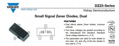
Thanks, Hugh - I will include the D23C15-E3-08GICT-ND dual Zener in my build.
Attached is a pic from the datasheet. The 2 legs on the same side are both Anodes - can you confirm it is these we connect to the Gate & Source of each MOSFET?
Hi X,
Given the pic of the dual-Zener that I have attached, can you tell me whether the connections you made for V101 on your Snubber PCB are compatible with the dual-Zener?
And thank you for explaining that the zener shown between Source & Gate is internal to the MOSFET.
But in relation to the text on your Snubber schematic ... can I suggest - for consistency - you need to replace V102 & V103 with V141 & V142!
Andy
Attachments
Sometimes JPS64 design circuits for me that have many sub systems and layers of functionality. You will come to appreciate that 3 or 4 digit numbering lets clusters of functionality be clumped together. For example, the Yarra preamplifier main board is one such case (the number will tell you WHERE on the schematic your eyes should gaze): Blah, blah blah ....
X, please don’t post unnecessary schematics to further confuse us!!! The point has already been made.
Please focus here on the AN circuit and especially clarify the question about the output MOSFETs.
Last edited:
X, please don’t post unnecessary schematics to further confuse us!!! The point has already been made.
Please focus here on the AN circuit and especially clarify the question about the output MOSFETs.
Hi Francois,
This is done as an example to help, not to confuse.
Also, if your going to quote a post, please don’t edit it with your own comments.
“Blah, blah blah....”
“Originally Posted by xrk971 View Post
Sometimes JPS64 design circuits for me that have many sub systems and layers of functionality. You will come to appreciate that 3 or 4 digit numbering lets clusters of functionality be clumped together. For example, the Yarra preamplifier main board is one such case (the number will tell you WHERE on the schematic your eyes should gaze): Blah, blah blah ....”
Thanks, Hugh - I will include the D23C15-E3-08GICT-ND dual Zener in my build.
Attached is a pic from the datasheet. The 2 legs on the same side are both Anodes - can you confirm it is these we connect to the Gate & Source of each MOSFET?
Hi X,
Given the pic of the dual-Zener that I have attached, can you tell me whether the connections you made for V101 on your Snubber PCB are compatible with the dual-Zener?
And thank you for explaining that the zener shown between Source & Gate is internal to the MOSFET.
But in relation to the text on your Snubber schematic ... can I suggest - for consistency - you need to replace V102 & V103 with V141 & V142!
Andy
Spacing between pins 2-3 on SOT23 is 1.9mm and pads for the MELF diode are spaced by 3.0mm, so it is a bit short. However, you could scrape off some of the solder mask on one of the pads and it would fit just fine. Or you could just follow the directions I gave for setting the orientation of the standard MELF diodes as you only need to solder 4 of these. (The Cathode stripe faces the MOSFET body on the N channel and away for the P channel). I think setting the correct orientation is easier than scraping the solder mask off near the pads. Plus, the specified MELF diode is probably more robust.
Last edited:
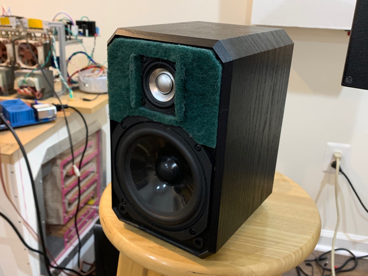
I just built a new set of speakers today and listening to them now with the Alpha Nirvana. They sound very nice - similar to the bigger 10F/RS225 FAST but smaller in a compact bookshelf form. These use the FR58EX full range and AC130F1 woofer in a FAST configuration. Uses a new passive crossover that I just designed a few days ago. I had the AC130F1's already and repurposed and old Boston HD5 cabinet.
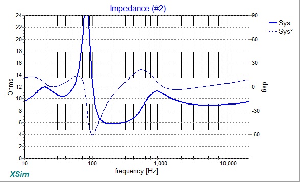
Although this XO dips down to 5.5ohms from nominal 8ohms, it sounds fine:
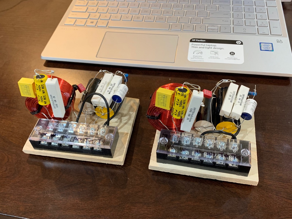
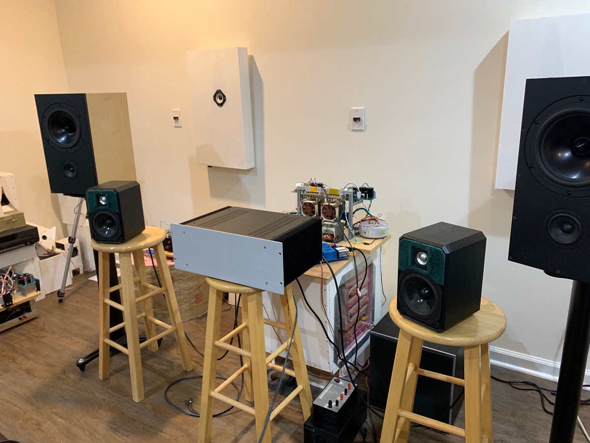
With the support of a subwoofer for stuff below 100Hz, the speaker works brilliantly.
Although this XO dips down to 5.5ohms from nominal 8ohms, it sounds fine:
With the support of a subwoofer for stuff below 100Hz, the speaker works brilliantly.
Last edited:
Spacing between pins 2-3 on SOT23 is 1.9mm and pads for the MELF diode are spaced by 3.0mm, so it is a bit short. However, you could scrape off some of the solder mask on one of the pads and it would fit just fine. Or you could just follow the directions I gave for setting the orientation of the standard MELF diodes as you only need to solder 4 of these. (The Cathode stripe faces the MOSFET body on the N channel and away for the P channel). I think setting the correct orientation is easier than scraping the solder mask off near the pads. Plus, the specified MELF diode is probably more robust.
Thanks, X.
Yes, if the Snubber PCBs aren't compatible with Hugh's suggested double diodes ... then we need to stick with the original single diodes.
Andy
I just built a new set of speakers today and listening to them now with the Alpha Nirvana. They sound very nice - similar to the bigger 10F/RS225 FAST but smaller in a compact bookshelf form. These use the FR58EX full range and AC130F1 woofer in a FAST configuration. Uses a new passive crossover that I just designed a few days ago. I had the AC130F1's already and repurposed and old Boston HD5 cabinet.
With the support of a subwoofer for stuff below 100Hz, the speaker works brilliantly.
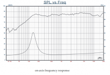
That's a huge (almost 15 dB) 10k resonance peak (reminds me of Lowther); must be audible even with a class A amp
Did you try SB65WBAC25-4? Looks much better.
FR58EX's factory curve looks much better too:
Attachments
X, can you advise?
I don't yet have my PCBs to look at - if I did ... all might be explained! But, in trying to create the 4R BoM, I am confused when I compare your 'As Built' schematic against Hugh's 4R cct diagram.
Hugh's 4R cct diagram has 'C1' (=10uF) ... whereas, in the same location your 'As Built' schematic lists:
* C102 = 10uF
* C103 = 0u1
* C104 = 10uF
* C105 = 10uF.
Does this mean that the PCB has space for 4 caps - totalling 30.1uF - instead of just 1 cap of 10uF?
(This also happens in at least one other location.)
Thanks,
Andy
I don't yet have my PCBs to look at - if I did ... all might be explained!
But, in trying to create the 4R BoM, I am confused when I compare your 'As Built' schematic against Hugh's 4R cct diagram.Hugh's 4R cct diagram has 'C1' (=10uF) ... whereas, in the same location your 'As Built' schematic lists:
* C102 = 10uF
* C103 = 0u1
* C104 = 10uF
* C105 = 10uF.
Does this mean that the PCB has space for 4 caps - totalling 30.1uF - instead of just 1 cap of 10uF?
(This also happens in at least one other location.)
Thanks,
Andy
Hi Andy,
In circumstances such as this, JPS64 gives multiple options for a given location.
As an example, for the input cap you can use a fancy 10uF film cap, a Wima 10uF box cap or a Silmic ll 10uF cap. The 0.1uF could be a film bypass if an electrolytic cap is used.
Your free to pick what you want to use
In circumstances such as this, JPS64 gives multiple options for a given location.
As an example, for the input cap you can use a fancy 10uF film cap, a Wima 10uF box cap or a Silmic ll 10uF cap. The 0.1uF could be a film bypass if an electrolytic cap is used.
Your free to pick what you want to use
Last edited:
That's a huge (almost 15 dB) 10k resonance peak (reminds me of Lowther); must be audible even with a class A amp
Did you try SB65WBAC25-4? Looks much better.
FR58EX's factory curve looks much better too:
Strange but my previous set did not have that huge peak. I see that peak on data from hdspeakerman’s data too. Something change in manufacturing. I think it is missing the rubber damping between the cone and dustcap. Here is data from 1st generation:
- Home
- Amplifiers
- Solid State
- Alpha Nirvana 39w 8ohm Class A Amp