abzug said:That picture reminds me of an ex.
... yeah. Don't you hate it when they walk off like that
")
Jan Didden
syn08 said:
Bob,
Some time ago, I tried myself to do some Hirata measurements (on some opamp based gain stages), using a MC1455 timer and MAX303 switches http://datasheets.maxim-ic.com/en/ds/MAX301-MAX305.pdf to generate a test signal from a dual DC power supply (I tried all four waveforms), multiturn pots as attenuators, and a HP3478A 5 1/2 digit multimeter to measure the output. I haven't played much though, as I concluded that the sensitivity is quite low. Almost anything better than a LM301 opamp gain stage showed nonlinearities buried in the noise.
Certainly only breadboarding the thing had an impact on the circuit performance, for sure a finished instrument would do much better. However, I am still skeptical regarding the resolution and sensitivity of this method, at least for power amps. I also find Hiraga's statement "It was found that high-quality amplifiers with a total harmonic distortion of 0.01-0.001% show a nonlinear distortion of more than 0.04%" at least confusing, as no correlation with the THD numbers is provided.
It could be a very good tool for evaluating speakers, though. I haven't tried this so far.
Hi syn08,
I re-familiarized myself with the patent and ended up with the same impression that it might be of limited sensitivity. I also think that there was an issue with whether or not the Hirata test applied the raw, fast-edged pulses to the amplifier, in which case its validity might be questionable (even the square wave of the DIM-30 and DIM-100 tests was filtered for this reason). I wish John could share more with us about his experience witht the Hirata box.
Cheers,
Bob
MOSFETs as drivers
I’m considering using a pair of heavily biased power MOSFETs in a bias spreader/NFB OPS arrangement to drive the bipolar output stage of one of my amp designs which consists of 20 parallel pairs of MJL3281/MJL1302.
At first glance Lateral MOSFET devices 2SJ201 / 2SK1530 looked like contenders, but now I’m not so sure. It seems these devices generally need a large amount for gate stopper resistance (~470 to ~680 ohms) to stop them from oscillating. This gate stopper resistance would seem to put an undesirably low, low pass pole in the combined driver/OPS frequency response.
HEXFET devices might be a better option for this application. My experience with HEXFETs is very limited (to LF power supply rail switching). Any ideas as to preferable types / complementary devices for this application and stabilisation techniques? Bob’s results with a series gate R plus RC to ground look promising.
Nelson Pass said:Personally I've never achieved satisfactory results driving
bipolar outputs with Mosfets, but I lack a good reason why
this should be so.
How much voltage, current and dissipation are you anticipating?
I believe MOS have exactly the opposite driver properties that are
required.
MOS driver = hiqh capacitance / low transconductance
BJT driver = low capacitance / high transconductance
When you think it through mos driver really doesn't have a lot going
for it.
T
Terry Demol said:
I believe MOS have exactly the opposite driver properties that are
required.
MOS driver = hiqh capacitance / low transconductance
BJT driver = low capacitance / high transconductance
When you think it through mos driver really doesn't have a lot going
for it.
T
A MOSFET driver at these power levels would be significantly earier to drive than and bipolar driver.
Nelson Pass said:Personally I've never achieved satisfactory results driving
bipolar outputs with Mosfets, but I lack a good reason why
this should be so.
How much voltage, current and dissipation are you anticipating?
This is a bit of an OTT design. The bipolar OPS has regulated rails of +/-~45V. Bias current is 5A, peak current is clamped at 120A.
Regulated rails of +/-55V are provided for the driver circuits and preceding circuitry
I would be mounting my PSU series pass transistors on the heatsink now on two 450mm X 30mm X 30mm lengths of square rod if Capral Aluminium wasn't closed on Saturdays
The design is being built in a modular fashion (PSU / OPS / driver board / input board / etc), so I will be able to easily experiment with different driver topologies, only having to redesign and substitute the driver board. The driver board is the only uncertainty in the design now.
Cheers,
Glen
Re: MOSFETs as drivers
Hi Glen,
I agree with you that gate stoppers do introduce an undesirably pole, but the 2SJ201 and 2SK1530 are vertical MOSFETs and can be used with smaller gate stoppers.
Cheers, Edmond.
G.Kleinschmidt said:[snip]
At first glance Lateral MOSFET devices 2SJ201 / 2SK1530 looked like contenders, but now I’m not so sure. It seems these devices generally need a large amount for gate stopper resistance (~470 to ~680 ohms) to stop them from oscillating. This gate stopper resistance would seem to put an undesirably low, low pass pole in the combined driver/OPS frequency response.
[snip]
Hi Glen,
I agree with you that gate stoppers do introduce an undesirably pole, but the 2SJ201 and 2SK1530 are vertical MOSFETs and can be used with smaller gate stoppers.
Cheers, Edmond.
Re: Re: MOSFETs as drivers
Also, now slightly off topic , after a gazillion design changes and flip-flops I have now actually finalised the design of my amp, deciding to forgo TMC, EC and all that fancy stuff (not the 1kW class A amp, which is another project). I have decided to just put my 12W amp topology with its 1k load resistor “crippled VAS” on steroids as an exercise to see just how good I can make it.
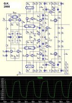
Shown below is an almost finished drawing of the input stage circuit board. With the compensation optimised for a 1MHz unity loop gain frequency, the front end simulates ~700ppb THD-20 driving 80Vp-p with an ideal output stage, and passes a 500kHz full amplitude squarewave as shown below
BTW, in your pretty PMP amp I notice that you use 220 ohm / 100 ohm gate stoppers for the 2SK1530 / 2SJ201. How come not the lower value gate stopper with the RC to ground?
Cheers,
Glen
Edmond Stuart said:
Hi Glen,
I agree with you that gate stoppers do introduce an undesirably pole, but the 2SJ201 and 2SK1530 are vertical MOSFETs and can be used with smaller gate stoppers.
Cheers, Edmond.
Also, now slightly off topic
, after a gazillion design changes and flip-flops I have now actually finalised the design of my amp, deciding to forgo TMC, EC and all that fancy stuff (not the 1kW class A amp, which is another project). I have decided to just put my 12W amp topology with its 1k load resistor “crippled VAS” on steroids as an exercise to see just how good I can make it.Shown below is an almost finished drawing of the input stage circuit board. With the compensation optimised for a 1MHz unity loop gain frequency, the front end simulates ~700ppb THD-20 driving 80Vp-p with an ideal output stage, and passes a 500kHz full amplitude squarewave as shown below
BTW, in your pretty PMP amp I notice that you use 220 ohm / 100 ohm gate stoppers for the 2SK1530 / 2SJ201. How come not the lower value gate stopper with the RC to ground?
Cheers,
Glen
Attachments
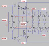
G.Kleinschmidt said:OK, here is what I have come up with for a VMOS driver. Nice and simple. The 20 pairs of output transistors run a bias current of 250mA each for 5A total bias.
Comments?
Looks a bit beefy for a Blowtorch pre amp OP.
Then again maybe you could call it the welding amp
Thread split?
T
Terry Demol said:
Looks a bit beefy for a Blowtorch pre amp OP.
Then again maybe you could call it the welding amp
Thread split?
T
Disregard my last reply, very late night, brain not engaged.
WRT MOS driver, yes I can see for driving 20 x OP BJT's it is a
very good option.
Question - Glen, why so much bias current? Why not concentrate on
the real challenge of ultra linear class AB? Much more fun than this
apparent overkill and waste.
T
Terry Demol said:
Disregard my last reply, very late night, brain not engaged.
WRT MOS driver, yes I can see for driving 20 x OP BJT's it is a
very good option.
Question - Glen, why so much bias current? Why not concentrate on
the real challenge of ultra linear class AB? Much more fun than this
apparent overkill and waste.
T
LOL
This is class AB! Just high bias class AB
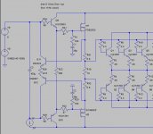
The idea is looking good so far, except that I had to add a pair of resistors (R91 and R91 in the pic attached) to compensate for the higher Vbe (about 100mV) of the small signal bias-spreader/temperature compensating transistors over the power output devices.
Also, Andy and Edmond, I've been too stupid so far to figure out how to get your modified 2SK1530/2SJ201 models working in LTspice. I keep getting error messages.
Cheers,
Glen
Oh, and another question before I go to eat pizza - where can I get 2SK1530's and 2SK201's from in low quantities????
Attachments
Hmm......
I think I may have found a possible mechanism for Nelsons complaint about MOSFET drivers for BJT's.
But before I get to that:
R91 and R92 (as described in my previous post) fixes one problem, but worsens another. When slewing at only 80V/uS the peak base current of the 20 output pairs peaks at 3A (mostly due to input capacitance of the BJT's).
The voltage developed across R91 and R92 by this base current, combined with the rise in Vgs for the MOSFETs, forces the driver stage to operate in class AB.
Now:
I can get rid of R91 and R92 and implement a more elaborate bias spreader circuit to compensate for the higher Vbe of the bias spreader feedback transistors, but that still doesn't get around the problem of the rise in Vgs of the MOSFETs, which will always force class AB operation of the MOSFET driver under fast slewing operation.
Referring to my previously attached schematic, the voltage developed across R19 is only small - a little higher than two Vbe junction drops. Once this voltage of approximately 1.4V is exceeded by the rise in Vgs for the MOSFET doing the driving at the time, the other will be cut off.
I hope I explained that clearly. I'm pretty sure it's right
This seems to me to be a major disadvantage of using MOSFET drivers for high power bipolar transistors output stages, and pretty much rules out the use of any simple bias spreader circuit if class A operation of the driver stage is desired under all operating conditions.
John?
AndrewT said:how does using BJT as a driver solve this ClassAB drive?
Easy - Unlike Vgs, Vbe doesn't have a delta >1.4V.
So, despite the fact that one driver BJT at any instant may be conducting huge peak base currents for its half of the output devices, the other driver transistor will never actually be forced into cut off.
- Home
- Amplifiers
- Solid State
- Bob Cordell Interview: BJT vs. MOSFET