you are concerned about temperature. Measure the temperature. Your fingers are a better measuring instrument than your ears.
No, in this thread here, I refer to bias current. temperature is quite clear in the other thread.....no more than 65W!!! I just use that as a guide line.
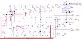
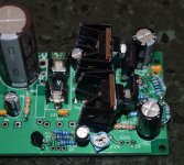
To put into perspective, attached is my schematic, layout and partially stuffed board.
I use Diamond 3EF with CCS for the first stage. I don't know what is class A pre-driver or driver. I use enough current through the two stages that I don't expect any of the transistor be turn off during the swing.
From the layout, you can see I have the NPN pre-driver and the PNP driver screwed together with a small heat sink on the right side of the picture so the drift of the 2Vbe canceled and track. I also have the bias spreader transistor (not stuffed on the board, but you can see the drawing of the pcb plot) bolted onto one of the MJL to get very close temperature tracking.
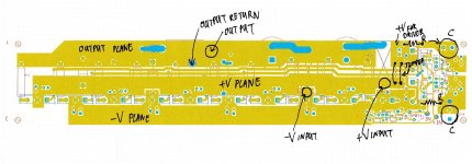
I have ground plane, two power planes and output plane. I have 0.1u and 10uF bypass cap right at the collector of all the power transistors and drivers. The power transistors are alternate NPN, PNP so the large current stay local. You can see only 4 long traces, two driving traces to all the power transistor and two input signals from the IPS/VAS board that drive the bias spreader and first pre-drivers. All other traces are made almost point to point. there is minimal ground plane under the two driver traces and output plane to minimize the capacitance loading. The ground plane is shown in the picture of the stuffed board.
I prefer diamond so I can compensate two of the Vbe. With the bias spreader mounted right on the big transistor, I think I got the temperature drift covered.
I also have two SS relay in parallel for speaker protection. The fault detector board is still in fab, be back in 2 wks.
As you can see, all you trouble makers made me pull out all the 0.12ohm. Another 3wks to wait for the 0.22ohm to ship from China.
I use Diamond 3EF with CCS for the first stage. I don't know what is class A pre-driver or driver. I use enough current through the two stages that I don't expect any of the transistor be turn off during the swing.
From the layout, you can see I have the NPN pre-driver and the PNP driver screwed together with a small heat sink on the right side of the picture so the drift of the 2Vbe canceled and track. I also have the bias spreader transistor (not stuffed on the board, but you can see the drawing of the pcb plot) bolted onto one of the MJL to get very close temperature tracking.
I have ground plane, two power planes and output plane. I have 0.1u and 10uF bypass cap right at the collector of all the power transistors and drivers. The power transistors are alternate NPN, PNP so the large current stay local. You can see only 4 long traces, two driving traces to all the power transistor and two input signals from the IPS/VAS board that drive the bias spreader and first pre-drivers. All other traces are made almost point to point. there is minimal ground plane under the two driver traces and output plane to minimize the capacitance loading. The ground plane is shown in the picture of the stuffed board.
I prefer diamond so I can compensate two of the Vbe. With the bias spreader mounted right on the big transistor, I think I got the temperature drift covered.
I also have two SS relay in parallel for speaker protection. The fault detector board is still in fab, be back in 2 wks.
As you can see, all you trouble makers made me pull out all the 0.12ohm. Another 3wks to wait for the 0.22ohm to ship from China.
Attachments
Last edited:
Can't seem to wrap my head around how your EF3 will behave thermally.
This post - http://www.diyaudio.com/forums/soli...f-hybrid-triple-any-pointers.html#post1906120
Shows the CCS/drivers as the second stage .
Normally , it is good to leave the predrivers to ambient. They use little
current and don't affect the co-efficient much.
the example in the post cancels the driver stage vbe , leaving the
pre's and outputs. The voltage spread will be that of an EF3 , but
Vbe will be just the outputs (and a tiny bit of the pre-driver).
You will just have to run your design and see where it falls.
The simulator sucks at thermal modeling - I model Tc mostly in my head !
(opposing similar devices - two Tc's cancel).
OS
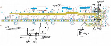
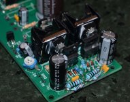
As you can see in my schematic, I have the Q8 KSA1381 and Q7 2SC2837 screwed together with thermal grease onto a small individual heatsink. The Vbe of the two canceled out on the first pass. More important is because they are bolted together and isolated from the main heatsink, the delta Vbe with temperature cancel as one goes -2mV/deg and the other goes +2mV/deg. I don't think you can make thermal response faster than this.
So I have only the big output transistor to compensate. That I layout so the bias spreader Q9 is bolted right on top of one of the big power transistor Q17. It's not going to be nearly as good as the NJL, but I doubt you can get faster thermal response if you put the bias spreader onto the main heatsink where heat has to travel over through the heatsink.
The spreader is for 2 Vbe of the power transistor instead of 6Vbe. More importantly, it's not even the Vbe that is important, you can always adjust the pot to compensate. It's the dynamic thermal response that I am after.
It's hell to layout this board. Took me like 3 days to make this happened. Only thing I am not happy is I should have done it so I have power transistor top and bottom of the pcb instead of one roll. I have a wide heatsink, it is more efficient to have transistor on both end of the pcb. I can either make the pcb shorter OR better yet, easily fit two more pairs of transistors.
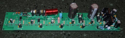
Attached are two close up pictures showing the pre-drivers and the drivers bolted together.
So I have only the big output transistor to compensate. That I layout so the bias spreader Q9 is bolted right on top of one of the big power transistor Q17. It's not going to be nearly as good as the NJL, but I doubt you can get faster thermal response if you put the bias spreader onto the main heatsink where heat has to travel over through the heatsink.
The spreader is for 2 Vbe of the power transistor instead of 6Vbe. More importantly, it's not even the Vbe that is important, you can always adjust the pot to compensate. It's the dynamic thermal response that I am after.
It's hell to layout this board. Took me like 3 days to make this happened. Only thing I am not happy is I should have done it so I have power transistor top and bottom of the pcb instead of one roll. I have a wide heatsink, it is more efficient to have transistor on both end of the pcb. I can either make the pcb shorter OR better yet, easily fit two more pairs of transistors.
Attached are two close up pictures showing the pre-drivers and the drivers bolted together.
Attachments
Last edited:
Nice diamond triple Alan! I use my version with the one point input from the VAS and different thermal comensation... It sounds very "transparent" , lower bias (65mA) and easy to try diffrent input stages.
To Bob Cordell : Have you made the actual working protos from the schematics of diamond triple from your book?
To Bob Cordell : Have you made the actual working protos from the schematics of diamond triple from your book?
So I have only the big output transistor to compensate. That I layout so the bias spreader Q9 is bolted right on top of one of the big power transistor Q17. It's not going to be nearly as good as the NJL, but I doubt you can get faster thermal response if you put the bias spreader onto the main heatsink where heat has to travel over through the heatsink.
You are correct. Putting the bias spreader on the heatsink will give you worse thermal tracking. Taking your layout, and completely surrounding the output device + bias spreader with insulating foam should improve thermal performance by minimising tracking errors (the thermal insulation forces all heat from the output device to go via the tab to the heatsink, minus the very small amount to heat the bias spreader).
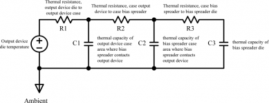
One thing that’s not clear to me is how best to maximise tracking speed. To a first approximation, the electrical equivalent circuit model of the bias spreader mounted on top of the output device and then surrounded in insulating foam, is as shown in the attached image. To maximise tracking speed we need the RC time constants to be as small as possible. R1 we can’t do anything about. R3C3 should be constant regardless of type of bias spreader transistor used, as a device with a larger die will have smaller R3 and larger C3, whilst a device with a smaller die will have larger R3 and smaller C3. What interests me is the effect of the bias-spreader case type on C1, R2 and C2.
Compare using here a TO92 to a TO126 with exposed metal tab:
For the TO92, C1 will be less (good) as the contact area is smaller, but R2 will be larger (bad). C2 is the big unknown for me. My hunch is that C2 is smaller for the TO92 due to the smaller size, but the material properties are important here and I don’t know the specific heat capacity or masses of the metal tab of the TO126 or the plastic body of the TO92. It’s a question I’d love to have time to answer experimentally but I just don’t have the time

Attachments
One thing I can think of to even speed up the transfer speed ( lower the thermal resistance and capacitance). If I wrap the power transistor Q17 with Indium foil that wrap from the bottom metal around the top before bolting onto the heatsink. The Indium is soft metal that actually mate with the surface when screwed tight. It help to transfer the heat from the bottom metal of the big transistor to the top, to the bias spreader. I don't think copper foil can do it as it does not mate with the surface. Putting grease make it even worst for the power transistor.
But this is getting very fancy and I don't know how much improvement you can get out of this. And one more thermal resistance of the Indium.
But this is getting very fancy and I don't know how much improvement you can get out of this. And one more thermal resistance of the Indium.
Even as I have builders that have put the output Vbe out on wires (for direct
output contact) , this might not be right for a EF3 compound vbe.
On the actual "beast" , I have noticed a "precompensation" in the
vbe's total response (to a sudden load).
Amps sits idle ... all of a sudden , a heavy load occurs. The driver HS
is very fast to react , secondary Vbe compensates before the main
one can. If the heavy load remains , the big HS's Vbe "catches up".
One would think that the outputs themselves would be over/under biased
going from zero to full load. Not the case , I've removed the load and
measured Re at this time - within a mV ( actually < .2-.3mv change).
Obviously , HK's engineers planned it this way.
They DID NOT mount the Vbe on the OP device ,
but put it 15mm to the side on the extrusion.
They DID sandwich the secondary Vbe between the drivers with a small
heatsink to increase speed of that Tc.
Alans design might have different thermal dynamics than this , I would
have to "abuse " it to find out.
PS - Did the same test to a HK990 with a T-trak pair , The OPS Vbe is the
internal diodes. Stayed <.1mv Re (in comparison).
OS
Final catch up of a few posts that I postponed due to end-of-financial-year pressure.
This should be a substantial improvement but there is still an external poloidal field and this is undesirable.
There's a few ways to cancel this field. Two opposed helixes would look nice.
Can I trademark "Double Helix" output inductors?
Best wishes
David
you can wind a air core toroid...still some ...field close in - but much reduced at distance vs cylindrical solenoid
It is easier to wind a solenoid and then bend it into a toroid. That is how I made this...
This should be a substantial improvement but there is still an external poloidal field and this is undesirable.
There's a few ways to cancel this field. Two opposed helixes would look nice.
Can I trademark "Double Helix" output inductors?
Best wishes
David
Maybe because Alan's output is not a 3EF.Can't seem to wrap my head around how your EF3 will behave thermally..............
It is a diamond followed by a 2EF.
What are Q12 & Q? supposed to do?
Are they required to be current sources into the diamond stage?
the Eline devices are much thinner than To92.....................One thing that’s not clear to me is how best to maximise tracking speed. To a first approximation, the electrical equivalent circuit model of the bias spreader mounted on top of the output device and then surrounded in insulating foam, is as shown in the attached image. To maximise tracking speed we need the RC time constants to be as small as possible. R1 we can’t do anything about. R3C3 should be constant regardless of type of bias spreader transistor used, as a device with a larger die will have smaller R3 and larger C3, whilst a device with a smaller die will have larger R3 and smaller C3. What interests me is the effect of the bias-spreader case type on C1, R2 and C2.
Compare using here a TO92 to a TO126 with exposed metal tab:
For the TO92, C1 will be less (good) as the contact area is smaller, but R2 will be larger (bad). C2 is the big unknown for me. My hunch is that C2 is smaller for the TO92 due to the smaller size, but the material properties are important here and I don’t know the specific heat capacity or masses of the metal tab of the TO126 or the plastic body of the TO92. It’s a question I’d love to have time to answer experimentally but I just don’t have the time
They will have less heat capacity and less thermal resistance Rth j-c.
I filed a dead To92 to find out how the internals related to the outside front face.
There is about 1mm of plastic between junction and front face. And about 2mm of plastic between junction and the curved surface.
I was able to go down to ~1mm thick before I hit any of the internal wiring.
Had I stopped by taking 0.5mm off the flat face and then taking the curved surface down to give a total thickness of 1.5mm, I reckon I would have an intact and working "thin" To92 roughly equivalent to an Eline.
Eline seems to be the answer for low capacity and low thermal resistance.
SMD sot23 is clearly even lower.
Maybe because Alan's output is not a 3EF.
It is a diamond followed by a 2EF.
What are Q12 & Q? supposed to do?
Are they required to be current sources into the diamond stage?
I thought it's still a 3EF, it's 3 stages of EF be it a diamond or not.
Q? and Q12 are 10mA current source as I want the CCS to active driving the second stage EF. It is not good to use resistor because when you get close to the rail, you looses drive capability with the resistor because there is not enough voltage drop across the resistor. I intend all the pre-drivers, drivers are always on even at full swing. I don't know whether you guys call this Class A drivers or not.
The two diodes are to prevent the CCS from saturating. It's the same idea of the schottky TTL that remove the base current to prevent the transistor from turning to forward forward bias.
Last edited:
I don't think your arrangement works as a current source.............................
Q? and Q12 are 10mA current source as I want the CCS to active driving the second stage EF.
it's not at full swing that where the device is full on, or near saturated that is the problem. It is at the opposite side when the device is almost turned off. The device must still be sufficiently on that it is still actively controlling the next stage. It is no good that it is not quite off (no Ic) and passing a near constant non zero current. That constant current effect means there is no active control and thus no ClassA. ClassA requires the device to operate/control over the full waveform............................... I intend all the pre-drivers, drivers are always on even at full swing. I don't know whether you guys call this Class A drivers or not.
I don't yet understand the anti-saturation and how to achieve it, but your diode layout looks OK.The two diodes are to prevent the CCS from saturating. It's the same idea of the schottky TTL that remove the base current to prevent the transistor from turning to forward forward bias.
Last edited:
Maybe because Alan's output is not a 3EF.
It is a diamond followed by a 2EF.
What are Q12 & Q? supposed to do?
Are they required to be current sources into the diamond stage?
Yes , you are correct. Alan made a hybrid. Just has 3 stages , like an EF3-
but it's not.
The one in my link isn't truly an EF3 , either - but closer.
I was "chicken" 4 years ago , did not build it.
Still ....will be interesting to see how Alan's works out.
OS
Look at R1 and R2, consider rail is 25V, current is about 4.55mA. voltage drop across R1 is 1.77V. this drive the base of Q?, it will be about 1V across R2, which drives 10mA through. Q? becomes a 10mA current source.I don't think your arrangement works as a current source
it's not at full swing that where the device is full on, or near saturated that is the problem. It is at the opposite side when the device is almost turned off. The device must still be sufficiently on that it is still actively controlling the next stage. It is no good that it is not quite off (no Ic) and passing a near constant non zero current. That constant current effect means there is no active control and thus no ClassA. ClassA requires the device to operate/control over the full waveform. I don't yet understand the anti-saturation and how to achieve it, but your diode layout looks OK.
I don't even follow what you are talking about. Q8 can drive going negative as it's a PNP EF, problem is when it tries to drive up, only the 10mA CCS by Q? is responsible to drive up.
The CCS by Q? is only responsible to drive Q7 only.
Q8 is never going to turn off, it's has 10mA in the diamond. Q7 is a big transistor for a driver. It is conducting 44mA through both R17 and collector of Q10. that is a lot of current capable to drive the power transistors, able to turn off the NPN transistors during the negative swing. If that's still not enough ( I don't think so), I can always increase the current. Q7 and Q11 should never turn off during operation. This is a simple circuit.
Last edited:
I agree that Alan's "hybrid" cleverly uses two opposed same sex transistors to compensate for Vbe changes as temperatures change.
Does this happen with all diamond stages followed by an EF?
Could that be why diamond stages are reputed to "sound good"?
I think all diamond stages can have the self compensation like what I do. It's the pain you have to go through in the layout to make it happen.
it passes current, in that respect it is a current source. It will be a pretty poor CCSLook at R1 and R2, consider rail is 25V, current is about 4.55mA. voltage drop across R1 is 1.77V. this drive the base of Q?, it will be about 1V across R2, which drives 10mA through. Q? becomes a 10mA current source.
You are now talking about not turning off. That is the condition you must ensure when the swing is at the opposite extreme. And consider it when the reactive load is demanding much more current than a resistive test load.I don't even follow what you are talking about. Q8 can drive going negative as it's a PNP EF, problem is when it tries to drive up, only the 10mA CCS by Q? is responsible to drive up.
The CCS by Q? is only responsible to drive Q7 only.
Q8 is never going to turn off, it's has 10mA in the diamond. Q7 is a big transistor for a driver. It is conducting 44mA through both R17 and collector of Q10. that is a lot of current capable to drive the power transistors, able to turn off the NPN transistors during the negative swing. If that's still not enough ( I don't think so), I can always increase the current. Q7 and Q11 should never turn off during operation. This is a simple circuit.
If you are using 25Vpk into 4ohms then peak output current should be around 20Apk. Can you simulate this condition? and see that the transistors are still actively controlling in ClassA manner.
it passes current, in that respect it is a current source. It will be a pretty poor CCSYou are now talking about not turning off. That is the condition you must ensure when the swing is at the opposite extreme. And consider it when the reactive load is demanding much more current than a resistive test load.
If you are using 25Vpk into 4ohms then peak output current should be around 20Apk. Can you simulate this condition? and see that the transistors are still actively controlling in ClassA manner.
25Vpeak into 4 ohm is only 6.25A peak, not 20A. Even 40V rail, it's only 10A peak.
I don't know which one turns off you are talking about. If you are referring to Q7 during negative swing. It's Q11 that pulling down, Q7 really does not have to do much work in pulling down. R17 is pulling the base of all the NPN power transistor down. You have 44mA of drive to pull the base of the 5 NPNs down. I think I am using a lot higher current than most designs I've seen. I use a 39ohm resistor R17 and add 10mA on top. that's high current by any respect. If this still turns off, most other designs are even worst.
If that really happens, it's very easy to increase current of Q? and Q12 to say 20mA to add another 10mA.
Last edited:
- Home
- Amplifiers
- Solid State
- Bob Cordell's Power amplifier book