You have to learn a new trick. Flood al pins with masses of solder using a wide solder tip. So you can heat all pins simultaneously and remove the chip wihtout damaging any pads. Works nice for me even with soic24 - I removed and re-used them that way successfullyHi Mr. Cordell
Ha ha, try removing a SOIC8 and replace with a new one. Then come back and talk!!!
Last edited:
..................... And consider it when the reactive load is demanding much more current than a resistive test load.
If you are using 25Vpk into 4ohms then peak output current should be around 20Apk. Can you simulate this condition? and see that the transistors are still actively controlling in ClassA manner.
Reactive speakers demand much higher currents when presented with fast transients.25Vpeak into 4 ohm is only 6.25A peak, not 20A. Even 40V rail, it's only 10A peak.................
Typically 150% for a bass only driver with no crossover.
But exceeding 300% for a 2way crossover type full ranger.
Tests have been reported showing rare music events exceeding 500% cf the nominal impedance of the speaker.
R.Cordell and D.Self have shown the transient current effects when using artificial waveforms. You have been quoting from both authors, presumably you have read the relevant sections.
I cannot tell you for sure. I can only tell you I looked at a lot of schematics, I yet to see any drivers stage run as high current as my design of 44mA. Most runs below 30mA. If I have problem, most others will have bigger problem. I choose this high current for the very reason. I use a 150W 2SC2837 as driver transistor to over kill the drive to ensure I can drive well. the pair of drivers are 150W 60MHz transistors with guaranty beta of over 50.
Also, I use 5 pairs of output transistors. This is way overkill in any respect. 5 pairs of 200W transistors and I design for 40V rail max. With the MJL, I will never see beta droop due to large current. Even if I take your word of 20A peak, that's only 4A per transistor. Even I am going for Oliver's optimization and use 0.22ohm Re, I am still gunning for 120mA per pair or 1.2A Class A current to give 2.88W of class A power.
If I have to worry about running out of steam, can you imagine most of the other amps.
Last edited:
the Eline devices are much thinner than To92.
They will have less heat capacity and less thermal resistance Rth j-c.
I filed a dead To92 to find out how the internals related to the outside front face.
There is about 1mm of plastic between junction and front face. And about 2mm of plastic between junction and the curved surface.
I was able to go down to ~1mm thick before I hit any of the internal wiring.
Had I stopped by taking 0.5mm off the flat face and then taking the curved surface down to give a total thickness of 1.5mm, I reckon I would have an intact and working "thin" To92 roughly equivalent to an Eline.
Eline seems to be the answer for low capacity and low thermal resistance.
SMD sot23 is clearly even lower.
Thanks for this.
You helped me realise that I made a mistake. In the previous diagram, transistor die and packaging do of course have an effect on the R3C3 time constant. R3 depends on both the size of the die and the packaging, whereas I was considering only the effects of the die size. As you say, devices with a thick layer of plastic from die to case, but with all other things being equal, will have higher R3.
So, the bias spreader transistor type (die size) and case style will together affect C1, R2, C2, R3 and C3.
Last edited:
Look at R1 and R2, consider rail is 25V, current is about 4.55mA. voltage drop across R1 is 1.77V. this drive the base of Q?, it will be about 1V across R2, which drives 10mA through. Q? becomes a 10mA current source.
Why are you using this arrangement and not something more “conventional” where you have something with much lower dynamic impedance connected to the transistor base-emitter, such as series connected diodes, LED, zener, or bandgap ref? What’s the output impedance of your “constant” current source and are there benefits to it being (presumably) relatively low?
I cannot tell you for sure. I can only tell you I looked at a lot of schematics, I yet to see any drivers stage run as high current as my design of 44mA. Most runs below 30mA. If I have problem, most others will have bigger problem.
None of them would have a "problem". Even a <10ma biased class A driver
stage would always stay class A. Even at 500W into a 1R load , regardless
of "droop". (below)
As the signal approaches 0V , only the current needed for Re needs to pass.
As the excursion approaches the rail , all the drivers current flows through
the base stoppers minus what is needed for the Re (to stay in A).
At least this is the way with a true EF3 ??
In that simulation , the NPN driver emitter plotted 310ma for that exaggerated
50A , 301ma went to the NPN output base stoppers.
OS
Attachments
In another thread , "Ayrton-perry" was mentioned.
..."Double helix" look's similar.
More like a mirror reflection, similar but opposite, I don't want to cancel out the inductance instead I want it to be maximised.
...currents when presented with fast transients.
...
Tests have been reported...rare music events...500% cf the nominal impedance of the speaker.
Where? The best tests I have seen were by Eric Benjamin, one of the senior Dolby people, published in JAES.
Didn't show it to happen on real music.
Didn't D.Self say that his casual tests, inspection of music waveforms on an oscilloscope, did not show any waveforms that looked even close to the required sharp transitions?R.Cordell and D.Self... authors, presumably you have read the relevant sections.
Best wishes
David
Last edited:
None of them would have a "problem".
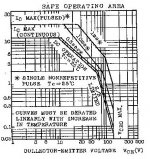
What's the point of using 100W power devices as drivers ?
fT of <15MHz at 44 mA, a TO-220 Toshiba does >40MHz at 10mA.
SOA example of a power device that's been used as a driver in a 200W serial manufacture amp, over 30MHz fT at 44mA.
(deepest excuses for the tongue in cheek part
 )
)Attachments
Last edited:
Why are you using this arrangement and not something more “conventional” where you have something with much lower dynamic impedance connected to the transistor base-emitter, such as series connected diodes, LED, zener, or bandgap ref? What’s the output impedance of your “constant” current source and are there benefits to it being (presumably) relatively low?
Are you referring to using R1 and R3 as voltage divider instead of using LED or zener to set up 1.7V at the base of "Q?"?
Good question!!! I can use either way and it does not matter. I drive 4.5mA through the divider so I have plenty of current for the base of Q?. So it really does not matter. I definitely do not want to use zener, for one, I only need 1.7V, and secondary, don't use zener, they are very noise, it pops. You always have to have a big cap to shunt it to quiet it down. Using a LED has no advantage as it's the 4.5mA drawn from R3 that keep Q? on.
About the two diodes, it is important to make sure Q? never saturates. The idea is exactly the same as Schottky TTL idea, D2 is used to rob base current of Q? to prevent Q? from going above the voltage on the base. I have to use D3 as I cannot use Shottky diode for D2. The collector of Q? can swing 2 times rail voltage, I need to use normal diode. But normal diode has 0.7V drop and I need D3 to drop 0.7V to cancel out the drop of D2. So theoretically the collector voltage of Q? will never go above the base.
What's the point of using 100W power devices as drivers ?
fT of <15MHz at 44 mA, a TO-220 Toshiba does >40MHz at 10mA.
SOA example of a power device that's been used as a driver in a 200W serial manufacture amp, over 30MHz fT at 44mA.
(deepest excuses for the tongue in cheek part
The devices I use for driver is 60MHz device with 160pF Cob. I want the size so it can survive even without heatsink. It is more important for me not to have them on the main heatsink so I don't get huge temp swing. At the time of design, I have no idea whether I can find a heatsink for them. So I use a huge transistor that can dissipates 2W without any heatsink. turn out I am right, I make the two drivers too close and I can only use a tiny heatsink. I doubt the arrangement I have now can handle over 3W with the tiny heatsink.
I design with very high slew rate in mind. I want to make sure I have beefy devices capable to do that easily. I have every plan of going to Ostripper's thread and work on the CFA IPS/VAS next. I am going to design a CFA IPS/VAS board next to pair up with this OPS board and expect to get over 1MHz bandwidth. That's why it never cross my mind to go 2EF.
On the IPS/VAS board, I lay the two VAS transistor down, create copper planes on both top and bottom under the trasistors, putting plenty of VIAs to stitch the two copper planes to get good thermal conductance and serve as heatsink. I am running 10mA on the VAS, It is a push pull VAS, I expect it to have very high slew rate driving a very light load of a 3EF diamond OPS. everything is gear for very high slew rate.
Last edited:
None of them would have a "problem". Even a <10ma biased class A driver
stage would always stay class A. Even at 500W into a 1R load , regardless
of "droop". (below)
As the signal approaches 0V , only the current needed for Re needs to pass.
As the excursion approaches the rail , all the drivers current flows through
the base stoppers minus what is needed for the Re (to stay in A).
At least this is the way with a true EF3 ??
In that simulation , the NPN driver emitter plotted 310ma for that exaggerated
50A , 301ma went to the NPN output base stoppers.
OS
Thanks
When Andrew asked this question, I immediately reference your circuits to see how much current you use as you are famous in extremely high slew rate and fast design. Ha ha, I downloaded a few of your schematic as reference. I have every intention to join your thread when I design a CFA IPS/VAS board. I way over kill on this OPS so it's ready to work with a CFA front end. I'll be on your thread when the time comes!!!
I am still learning how to walk here, leave the running later. Enough nuance to learn everyday talking here already. I really appreciate the comments from you guys. I expect to have a lot of special knowledge in audiophile electronics, but I am still surprised how much there is, things that I never have to consider in my career.
Thanks
Last edited:
Thanks
When Andrew asked this question, I immediately reference your circuits to see how much current you use as you are famous in extremely high slew rate and fast design. Ha ha, I downloaded a few of your schematic as reference. I have every intention to join your thread when I design a CFA IPS/VAS board. I way over kill on this OPS so it's ready to work with a CFA front end. I'll be on your thread when the time comes!!!
Thanks
There are "tricks" beyond this .. studied the HK680 , 220R Re - just 7ma.
Scope says it always stays A. Why so low ?
Toshiba 4793/1837 drivers plus the secondary Vbe run real cool until
you run 100W/4R. Big swing in temperature. This was planned to
make the bias spreader "fast".
If I ran hot (20-40ma) , a dynamic load would not have as great an effect
on the driver Vbe. I then chose 9ma ,
as I was using slightly larger (mt-100) drivers on a larger heatsink (same idle T). I'm a little
slower , but still <2 seconds.
The only real way to determine all this , is to run it on the table in front
of you and "do the deed".
PS - those small heatsinks on your drivers would overheat at even 20ma.
My builders had driver heat issues until I lowered current to <10ma. They
used 100mm x 100mm plates !
OS
What's the point of using 100W power devices as drivers ?
fT of <15MHz at 44 mA, a TO-220 Toshiba does >40MHz at 10mA.
SOA example of a power device that's been used as a driver in a 200W serial manufacture amp, over 30MHz fT at 44mA.
(deepest excuses for the tongue in cheek part
I'm using 2sc3263/sa1294 as driver. Whats wrong with them ?
Better Cob than MJE's. Way faster
I see what you mean , Ft-IE characteristics . Those sanken do
30mhz @ 20ma ... but that's a 12V plot. I think at 50-70V ,
things are different.
Still , way better than a MJE15032/33 pair. That datasheet don't
even plot Ft ???
I DO use the 4793/1837 pair for the Vfet option on my OPS board.
Those can also be used for 3 pair higher beta sanken OP's.
Still , tested the fastest CFA >250v/us on those big drivers. One
builder had my "bad designs" .... the EF3 output was a 30mhz
signal that interfered with his radio's (burned the zobel , too) !!
OS
There are "tricks" beyond this .. studied the HK680 , 220R Re - just 7ma.
Scope says it always stays A. Why so low ?
Toshiba 4793/1837 drivers plus the secondary Vbe run real cool until
you run 100W/4R. Big swing in temperature. This was planned to
make the bias spreader "fast".
If I ran hot (20-40ma) , a dynamic load would not have as great an effect
on the driver Vbe. I then chose 9ma ,
as I was using slightly larger (mt-100) drivers on a larger heatsink (same idle T). I'm a little
slower , but still <2 seconds.
The only real way to determine all this , is to run it on the table in front
of you and "do the deed".
PS - those small heatsinks on your drivers would overheat at even 20ma.
My builders had driver heat issues until I lowered current to <10ma. They
used 100mm x 100mm plates !
OS
ostripper, one request for you `cos I have my doubts....
")
Would you apply full swing sqare wave 1KHz at input of your EF3 buffer and print the simulation screen for a driver npn or pnp emitter current on the classic 8 Ohms load and post the picture here please?
ostripper, one request for you `cos I have my doubts....
Would you apply full swing square wave 1KHz at input of your EF3 buffer and print the simulation screen for a driver npn or pnp emitter current on the classic 8 Ohms load and post the picture here please?
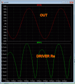
Look at them I spikes with a 250v/us CFA. See why I like the robust
driver pair ?
Builders have approached this level on the bench. They tried it at 20k
and most zobel's can't take it
.PS - because of the spikes , hard to see the average P/N current ... It's about 80ma Ie
per device.
OS
Attachments
Last edited:
Look at them I spikes with a 250v/us CFA. See why I like the robust
driver pair ?
Builders have approached this level on the bench. They tried it at 20k
and most zobel's can't take it
OS
That is what I talk about... I don`t know is that the model / simulator error or these spikes are real? Have you tried this on the scope? You could look even at the bases of the EF3 predrivers, the situation is the same. Lower rise time of the square wave generator doesn`t make the difference it is not a high SR related I think...
I run my drivers at 100mA , that is the simulator worst case I found enough ,it`s fool proof and that is with sine input and complex load. I don`t think these spikes are that realistic or every of our amps work in class AB
Last edited:
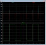
(below) is the fastest that EF3/big drivers can do.
The OPS is the limiting factor at 300V/us. Those toshiba's can go 50+V/us
faster.
Anatech , yes ... this is the big "CFA fiasco" . A standard
150-220pF input filter cap will make the VFA the same as a CFA.
Borgo , builders have seen the spikes and blew to-220's.
The 150W to-3P's can actually handle this abuse.
Slower 21193/4 outputs will go into X conduction (and blow).
The 3503/1381 - 2sc3263/sa1294 - njw0281/0302 EF3
is quite durable and can handle any input stage.
Edit - wrong pix ... toshiba's will do 350V/us , they
are faster in this ef3.
OS
The OPS is the limiting factor at 300V/us. Those toshiba's can go 50+V/us
faster.
Anatech , yes ... this is the big "CFA fiasco"
. A standard150-220pF input filter cap will make the VFA the same as a CFA.
Borgo , builders have seen the spikes and blew to-220's
.The 150W to-3P's can actually handle this abuse.
Slower 21193/4 outputs will go into X conduction (and blow).
The 3503/1381 - 2sc3263/sa1294 - njw0281/0302 EF3
is quite durable and can handle any input stage.
Edit - wrong pix ... toshiba's will do 350V/us , they
are faster in this ef3.
OS
Attachments
Last edited:
That is what I talk about... I don`t know is that the model / simulator error or these spikes are real? Have you tried this on the scope? You could look even at the bases of the EF3 predrivers, the situation is the same. Lower rise time of the square wave generator doesn`t make the difference it is not a high SR related I think...
I run my drivers at 100mA , that is the simulator worst case I found enough ,it`s fool proof and that is with sine input and complex load. I don`t think these spikes are that realistic or every of our amps work in class AB
Who would play a 200W square wave through their speakers?
The predrivers see very little of this "spike" , they are not class B
like the outputs , less Cob ... as well.
The outputs are the only semi's that are actually switching.
Total "overkill" !
OS
Are you referring to using R1 and R3 as voltage divider instead of using LED or zener to set up 1.7V at the base of "Q?"?Why are you using this arrangement and not something more “conventional” where you have something with much lower dynamic impedance connected to the transistor base-emitter, such as series connected diodes, LED, zener, or bandgap ref? What’s the output impedance of your “constant” current source and are there benefits to it being (presumably) relatively low?
Yes. I should have said transistor base-power rail, rather than transistor base-emitter.
Look at R1 and R2, consider rail is 25V, current is about 4.55mA. voltage drop across R1 is 1.77V. this drive the base of Q?, it will be about 1V across R2, which drives 10mA through. Q? becomes a 10mA current source.
Did you simulate this? According to LTspice (using a 2SA1930 model I built myself so I know it’s accurate) this arrangement will give you 21 mA for a 40 V rail.
BTW, 2SA1930 is EOL although availability still looks good so I guess they weren’t selling well. In the other polarity you are using the 2SC4793. The complementary part is 2SA1837. Is there a reason you are using 2SA1930 rather than 2SA1837?
Good question!!! I can use either way and it does not matter. I drive 4.5mA through the divider so I have plenty of current for the base of Q?. So it really does not matter. I definitely do not want to use zener, for one, I only need 1.7V, and secondary, don't use zener, they are very noise, it pops. You always have to have a big cap to shunt it to quiet it down. Using a LED has no advantage as it's the 4.5mA drawn from R3 that keep Q? on.
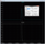
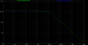
As it turns out, output impedance of your arrangement is higher than I expected, and actually is slightly higher at low frequency vs putting two 1N4148 in place of the 390R resistor. However, performance is slightly worse at higher frequencies (see attached - green trace is your arrangement, blue trace is “more conventional” arrangement, vertical axis is output impedance in Ω, horizontal axis is frequency in Hz).
One area where your arrangement is unquestionably worse is power supply rejection. Any variation in the power rail will appear across the current-setting resistor. Replacing the 390R resistor with 2 series 1N4148 and reducing the 100R to 36R gives a wider compliance range and 18 dB higher supply rejection.
Attachments
- Home
- Amplifiers
- Solid State
- Bob Cordell's Power amplifier book