I like Mr. Cordell's response to Alan's "learning". Truly a positive attitude.
With the few problems (magic smoke) on the hundreds of Badgers and
Slewmasters , I never had a condescending attitude and helped
them through it. One can even learn from a common mistake by the
builder and feed this back to the next (PCB) revision.
All the various threads that Mr. Cordell has contributed to are a learning
experience in themselves.
PS - Bob , I have some pretty "exotic" topologies that you might want
to cover. I have no real "prior art" on my Baxandall (super-pair)/cascode.
It has also been tested in the "real world" X100 now ..... perfected !
OS
Will appreciate all comments.
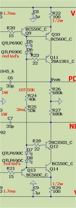
Nattawa , try the "exotic" VAS I just mentioned (below).
-self clamping
-beta enhancing
-ultra high Z
-Ivas trimmable (r24)
Superior to a Hawksford in EVERY way. You don't need
to bypass Re on the VAS to get sub PPM (below 2).
OS
Attachments
Thanks OS! PCB was ordered a year ago and prototyping is now underway. I'll definitely try your "exotics" at next revision. I've used "too many" transistors in the IPS/VAS already to bother two moreNattawa , try the "exotic" VAS I just mentioned (below).
OS

Attachments
Nattawa,
I see a bunch of smd on your board but those output devices are all so close together, don't you think you will have problems with heating of the center devices with all five pair populated?
Yes, I think I might. But I decided a smallest possible feedback signal loop was priority when put to layout. I use 0.33-ohm Re at OPS, and will use phase change thermal interface material to bring the Rth C-S down as much as possible. I would also consider soldering same gender OPS transistors on a copper bar heat spreader. And in a worst case scenario that all these do not work out, I just lift 2 of the 5 pairs. It's a +/-65V rail amp after all. The PCB is having IPS-VAS-OPS, and a solid state speaker relay on it and was intended to fit on a 10-inch width X 6-inch length heat sink, I wish I could do better in placing the power transistors.
Hi Bob and all,
(...)
Will appreciate all comments.
Hi Mr. Cordell
(...)
Can you tell me whether I am totally off?
First problem: Your style is, to me, rude and inconsiderate to all other forum members except perhaps those you are summoning for answers. Take a look above at how should a question be posted on a public forum. Your posting style effectively tells others "there's only one person I am interested in discussing with".
Second problem: people around are freely giving and taking advice and ideas. I would expect from somebody with 30 years of EE experience, tons of books read, patents owned and written, etc... to be able also to share something that others may find interesting. Instead, you are in a continuous demand mode, otherwise without any contribution to the general body of knowledge.
Sorry for the cold shower.
All I can say is that lower Re sound better, you should shift the bias current value when changing them but I can clearly hear that lower Re sounds better and I don`t have extra bad *** speakers. Also different Re value wants different bias current so you could get the best sound at crossover region, there is no magic number for bias current and you should go for the lower base stoppers also.
All that I noted I can hear at home without any measuring instrument but I listen in mono with 2 Ohms load (two paralleled 4 Ohm speakers)
All that I noted I can hear at home without any measuring instrument but I listen in mono with 2 Ohms load (two paralleled 4 Ohm speakers)
First problem: Your style is, to me, rude and inconsiderate to all other forum members except perhaps those you are summoning for answers. Take a look above at how should a question be posted on a public forum. Your posting style effectively tells others "there's only one person I am interested in discussing with".
Second problem: people around are freely giving and taking advice and ideas. I would expect from somebody with 30 years of EE experience, tons of books read, patents owned and written, etc... to be able also to share something that others may find interesting. Instead, you are in a continuous demand mode, otherwise without any contribution to the general body of knowledge.
Sorry for the cold shower.
So far, the only one here that is rude, sarcastic and unhelpful is you.
All I can say is that lower Re sound better, you should shift the bias current value when changing them but I can clearly hear that lower Re sounds better and I don`t have extra bad *** speakers. Also different Re value wants different bias current so you could get the best sound at crossover region, there is no magic number for bias current and you should go for the lower base stoppers also.
All that I noted I can hear at home without any measuring instrument but I listen in mono with 2 Ohms load (two paralleled 4 Ohm speakers)
Did you say you use 0.16ohm and have no problem?
I build another two OPS board and I ordered the 0.18ohm to experiment and see whether I can hear the difference.
Mono?
Thanks OS! PCB was ordered a year ago and prototyping is now underway. I'll definitely try your "exotics" at next revision. I've used "too many" transistors in the IPS/VAS already to bother two more
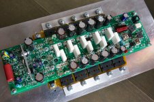
That looks REALLY sweet.
Even with "Virgin" aluminum , having the OP's close like that might make
for a "hot spot" (the middle pairs).
Chinese aluminum , I had as much as 3mv (higher bias) on the center
pairs.
That version of my OPS , I now use just 3 pair spread out double
spaced. No issue.
I'm curious whether the T-trak's have this errata ?
I spread my new slew OPS out to 5 pair across a 250mm extrusion.
My builder Still4given has his tightly packed 5 pair (and tested it for me).
He only gets about 1mV variation from middle to ends.
The smaller the heatsink the worse this little issue becomes.
OS
 Guys (you know who you are) take it down a notch, Bob C has made his position pretty clear, and the discussion can continue on its current basis without the sniping back and forth.. Attack the topic material, not each other. Thank you..
Yes, I think I might. But I decided a smallest possible feedback signal loop was priority when put to layout. I use 0.33-ohm Re at OPS, and will use phase change thermal interface material to bring the Rth C-S down as much as possible. I would also consider soldering same gender OPS transistors on a copper bar heat spreader. And in a worst case scenario that all these do not work out, I just lift 2 of the 5 pairs. It's a +/-65V rail amp after all. The PCB is having IPS-VAS-OPS, and a solid state speaker relay on it and was intended to fit on a 10-inch width X 6-inch length heat sink, I wish I could do better in placing the power transistors.
You can reduce the close proximity by cutting slits on the heatsink, between the transistors.
Gajanan Phadte
Yes, I think I might. But I decided a smallest possible feedback signal loop was priority when put to layout. I use 0.33-ohm Re at OPS, and will use phase change thermal interface material to bring the Rth C-S down as much as possible. I would also consider soldering same gender OPS transistors on a copper bar heat spreader. And in a worst case scenario that all these do not work out, I just lift 2 of the 5 pairs. It's a +/-65V rail amp after all. The PCB is having IPS-VAS-OPS, and a solid state speaker relay on it and was intended to fit on a 10-inch width X 6-inch length heat sink, I wish I could do better in placing the power transistors.
My design has 5 pairs, but I have it in a straight line, not that it's better. I have the transistor kind of tight also. But it all boils down to how much power are you trying to get out of. Also, you have not shown how the heat sink looks like, if it has long fins, nothing wrong with that.
I for one is not going for high power, I am more going for higher bias current. Even I am now going for Oliver's condition to get 26mV across the Re, I am still pushing to lower the Re and raise the current. I am planning to use +/-40V rail, BUT I am more interested to lower the rail if I can make it work with higher bias current to get more Class A power.
So the question is how much power you are going to want out of your amp? Remember even though it looks very tight, but you still have 5 pairs!!!! No point of eliminate two pairs and only use 3 pairs, just don't work them so hard. Remember, with 5 pairs, you have advantage of better SOA limitation. I never understand why people push so hard to stay with two or three pairs and worry so much about the SOA and resort to use "the" transistor.
Bottom line, if all else are equal, I'll take your tight 5 pairs over any others with two or three pairs if you want to get the same power output. You just create hot spot on the heat sink if you use less pairs.
Last edited:
Nattawa , try the "exotic" VAS I just mentioned (below).
-self clamping
-beta enhancing
-ultra high Z
-Ivas trimmable (r24)
Superior to a Hawksford in EVERY way.
Implementation of what is known as Boxall-Baxandall's (and some other authors) pair seems to be pretty tricky :
http://www.diyaudio.com/forums/solid-state/25172-baxandall-super-pair.html
My design has 5 pairs, but I have it in a straight line, not that it's better. I have the transistor kind of tight also. But it all boils down to how much power are you trying to get out of. Also, you have not shown how the heat sink looks like, if it has long fins, nothing wrong with that.
I for one is not going for high power, I am more going for higher bias current. Even I am now going for Oliver's condition to get 26mV across the Re, I am still pushing to lower the Re and raise the current. I am planning to use +/-40V rail, BUT I am more interested to lower the rail if I can make it work with higher bias current to get more Class A power.
So the question is how much power you are going to want out of your amp? Remember even though it looks very tight, but you still have 5 pairs!!!! No point of eliminate two pairs and only use 3 pairs, just don't work them so hard. Remember, with 5 pairs, you have advantage of better SOA limitation. I never understand why people push so hard to stay with two or three pairs and worry so much about the SOA and resort to use "the" transistor.
Bottom line, if all else are equal, I'll take your tight 5 pairs over any others with two or three pairs if you want to get the same power output. You just create hot spot on the heat sink if you use less pairs.
The heat will come from the constant current flow of the high bias current more than playing at high power. On a smaller heat sink the heat will travel horzontally away from the end devices. This can't happen as easily for the center devices. You still need to deal with this same issue.
My point in response to him is eliminating 2 pairs is not going to make it any better if he still use the same board on the same heatsink and want the same power output and total bias. It's likely to be even worst. Of cause if he can have a bigger heatsink and do a new pcb, that's a different story.The heat will come from the constant current flow of the high bias current more than playing at high power. On a smaller heat sink the heat will travel horzontally away from the end devices. This can't happen as easily for the center devices. You still need to deal with this same issue.
If he can live with lower total bias and lower power output, he can do the same thing with 5 pairs, no need to remove any of them.
It's really no point of talking about this as he did not specify the power dissipation requirement. We don't know what he plans to bias at.
Last edited:
That is very small because it's being divided by R1/(R1+R3). More importantly the current is driving into the emitter of the pre-driver Q8 which r'e = 2.6ohm. It's not going to make a difference.
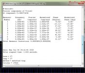
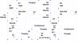
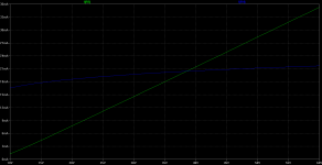
Please see attached schematic and graph comparing your arrangement to a “more conventional” arrangement. The setup here tests the current source current as the power rail varies from 10 to 60 V. Vce of the BJT is kept constant at 10 V for a fairer comparison. Green line is output current of your current source, blue line is output current of conventional design.
For those that have built diamond buffers - what do you all think? Do the current sources need to be “constant” current sources or is Alan’s arrangement just fine?
Attachments
My point in response to him is eliminating 2 pairs is not going to make it any better if he still use the same board on the same heatsink and want the same power output and total bias. It's likely to be even worst. Of cause if he can have a bigger heatsink and do a new pcb, that's a different story.
If he can live with lower total bias and lower power output, he can do the same thing with 5 pairs, no need to remove any of them.
It's really no point of talking about this as he did not specify the power dissipation requirement. We don't know what he plans to bias at.
Eliminating two pairs may and likely will make it better. It could be better to run three pair without the outer devices superheating the center device. There is a good possibility that the center device would run closer to the same temperature as the outer two devices and the overall power could be raised because there isn't a current hogging device in the set. There's also the more obvious point that having three pairs of devices idling at 26mA will produce 60% of the heat that 5 pairs of devices idling at the same current. There's more to power handling than just number of output devices is my point. Properly implementation is very important.
... an amp that has a mirror loaded, symmetric complementary IPS and a push-pull VAS, or Figure 7-10-ish circuit in Bob's book (Yeah, I admit I have poor resistance to eye candy symmetry in schematics).
...
Will appreciate all comments.
I have been reluctant to comment on this but you haven't had much response so here's my ideas.
First, the current mirror helper transistors seems undesirable. They add an extra pole and are usually detrimental to stability.
Bob adds them on p139 with the intention to improve the balance of the current mirror and match the potential drop of the EF assisted VAS.
Since you don't have an EF assisted VAS they offer no benefit in this circuit, only the stability downside and of course a little extra unneeded complexity.
Second, the LTP cascodes also seem undesirable. You have lowered the impedance into which the cascodes work with the 47K shunt resistor, which more or less defeats their purpose. And of course more complexity.
I did some simulations with Bob's resistor shunt solution and found it was not very robust to minor mismatches in LTP emitter resistor mismatch or transistor mismatch. It has no way to discriminate between Common Mode and Differential mode.
Hope that doesn't sound too critical, it's one of the few circuits in the book that I think needs to be re-examined.
Your circuit has cascodes on the VAS rather than EF assisted VAS so it should be less vulnerable, but I would recommend you try different sorts of mismatches and see how it balances.
You can use the spare transistors from the previous two comments to make a Common Mode Control Loop.
Or perhaps try Edmond Stuart's SuperTIS front end.
I also think your compensation may be vulnerable to component mismatch.
Bob does discuss this in his book and I think you should check this too.
I think a MIC works better for this application.
Actually I think it works better for most applications, but that's a different debate.
Best wishes
David
Last edited:
Implementation of what is known as Boxall-Baxandall's (and some other authors) pair seems to be pretty tricky :
http://www.diyaudio.com/forums/solid-state/25172-baxandall-super-pair.html
They did not get too far , did they ?
Quasi-sat of the BC550/560 as the super pair is the key to success.
Had it oscillate once with a very high OLG design , but it behaved
better than a Hawksford in that same design.
CLG and phase are stellar , drives an EF3 quite well. As with any cascoded
design , I would not drive LFET's or an EF2 directly with it.
(like so many horrible internet designs).
OS
- Home
- Amplifiers
- Solid State
- Bob Cordell's Power amplifier book