Imho, not the way it should be done, this cable is not good for that purpose.
Each the 3 signals of I2S should have the same care : having each is own gnd as return path, isolated enough by a spacing witch each I2S signal for each gnd not to be mixed between 2 I2S signals that share a same spacing with a gnd wire in between which could be at iso spacing !
For illustration : SG-N-SG-N-SG. S stands for Signal, G for Gnd return path, N for a spacing bigger than the distance between S&G or an inert trace more or cut if a pcb plane.
A global shielding has not really interest there, if exist should be just wirered on one side to gnd at the receiver side to avoid ground loop and mixed ground signals between the 3 I2S. One side connection allows shielding. But notice the shielding is not often for the signals but to avoid signals pollute close devices (EMI). Best practice is to make the shorter i2S path between the emitter and receiver (DAC chip). I2S was a protocol for CD players for short lengths.
UF-L wires allows each channel to have both its own gnd return path, keep the same impedance between boards and acts as a shelding for close I2S to be isolated from each others as they should be from each other on the circuitry by a proper spacing or a cutting or a copper trace cuted at one side. All the lengths between the emitter and receiver should be the same or close enough not to introduce timming issues with the three active signals. Texas Instrument has good application notes free ressources on this.
2" uf-l cables should be chosen over 4" that makes often length too much long between boards. Another good solution is the pins stacking as per Miro design with the little spidf board. As if it was the same board (which ultimatly is not, soldering joints are a nightmare)
if two rows connector are chosen the first row close to the pcb side should be Gnd, each Gnd vias farer between each other than the above row towards the inside of the pcb for the I2S signal (each I2S signal in front of his own vias Gnd, each Gnd vias far enough from each other)
It's a good practice if the uf-l must be direct to the dac chip to solder these uf-L pads near the dac chip with eventually space enough for a resistor in serie for bouncing stopping purposes.
Last edited:
Miro,
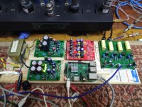
Just a quick update. Due to the current lockdown in Malaysia because of the increase in Covid-19 infections, I have had the time and opportunity to complete miro’s PCM56 layout. I too can confirm that it works perfectly. The glue logic for converting i2s to 16 bit EIAJ works as intended. The i2s is supplied by a Raspberry Pi 3.
As with the AD1862 board, the PCM56 dacs are powered from Trileru’s implementation of the Denoiser circuit for both LM317 and LM337. The PCM56 pcb is running on +/-5V rails and +/- 11.25 V rails. This is because, I used 2 10V Zener diodes from the adjust pin of the LM317 and LM337 to ground, relying on the constant current generated at the adjust pins of both regulators respectively. As for the +/- 5V rails I used 2 green leds in series as a voltage reference, again from the respective adjust pins to ground.
I have not used the op amp option for the output stage, but have used a variation of Nelson Pass’s D1 i/v stage, leaving out the source follower part and taking the output directly from the drain and coupled with a 6.8uF film capacitor. I made no changes to resistor values for the Nelson Pass’s D1 i/v stage. The same values were used. However, my implementation of the pcb for the Nelson Pass’s D1 i/v , enables me to try out both the IRF630 and IRF610 mosfets without having to rewire everything.
Thus far the dac is running on the IRF630 mosfets.
Because the Nelson Pass’s D1 i/v was designed for the PCM63 dac which has a 2 ma current output, I piggybacked 2 PCM56 dacs per channel to output 2 ma. The PCM56 dacs do run hot though.
I must say that the sound appears to be weightier than the AD1862, but the details in the highs appear subdued and less prominent.
I am not sure if this is because of the use of IRF 630 instead of IRF610, I am presently listening to whereas I used IRF610 mosfets in the D1 i/v stage for the AD1862.
The soundstage is equally wide, deep and open. All in, the dac sounds great, and I am well pleased with the effort. The old R2R dacs really make the current PCM1794, AD1955 and ES9018 dacs sound thin, puny and lifeless compared to the AD1862 and the PCM56P. Will try out the AD1851 and AD1860 dacs next, after I procure them. I also intend sometime in the future to power them from shunt regulators.
Many Thanks for the effort taken to layout the pcb's and providing the Gerber files. Great stuff.
Attachments
Imho, not the way it should be done, this cable is not good for that purpose.
Each the 3 signals of I2S should have the same care : having each is own gnd as return path, isolated enough by a spacing witch each I2S signal for each gnd not to be mixed between 2 I2S signals that share a same spacing with a gnd wire in between which could be at iso spacing !
For illustration : SG-N-SG-N-SG. S stands for Signal, G for Gnd return path, N for a spacing bigger than the distance between S&G or an inert trace more or cut if a pcb plane.
Oh dear, I have not implemented your recommendation. My PCM56 dac works though.


DIR9001 is available on mouser. It has the same quality as the WM8804 or WM8805 - tests were done by some guys.
On jitter side they are close, but some ultimate designers found the DIR9001 in a good layout wins as far the ears are concerned. I didn't make the test myself but trust the guy that told me as he designed my daily dac. It's like the CS8014 and CS8016, many prefer the first ! We have to remember some only rates chips with measurement as they rate dac chip on datasheets, but don't take the time of the proof test by designing and then hearing, too much hassles for them after the "good" measurement.
It's full of things like that here, like oh look the scope of my hypex amp, it beats everything on the scope, etc, etc... often such system sounds ...poor, ears direct biased class A by the eyes
")
FWIW & YMMV, as usual.
Last edited:
They both have their merits. I havent done any long term evaluation as yet. As I said, the AD1862 although a little leaner in presentation, sounds very open and clean. The highs as I had said appear to be finer. In terms of what the British refer to as PRAT, the AD1862's presentation tends more to induce foot tapping in the listener.
I suppose it is a matter of presentation, eg. I have both a Audio Research VT130 and Classic 30 power amps and in the picture is a hidden view of a Quicksilver GLA power amp. Although all 3 are tube based amps, the presentation is diametrically opposite. The Quicksilver is warm and weighty, whereas the Audio Research amps are fast, clean and leaner, with a sound closer to solid state; but with a tube midrange liquidity.
The same analogy is true of the PCM56 vs AD1862. Build both and enjoy the differences as your mood takes you.
One thing is certain though; either PCM56 or AD1862, sounds superior to the AD1955, PCM1794 and ES9018, Dacs which I have.
These are my 2 cents worth.
I intend to try out the AD1860 next and will report.
Thanks.
My experience with Miro’s AD1862 dac is that it’s very very sensitive and specific with only small changes of periferal parts around it. An opamp swap or other lytics near opamp gives an huge difference in sound I have never heard that big steps before. Sorry for my up and down responses here lol
With opa627 I am getting somewhere.
My non os cdp with glue logic I had pedja’s AD844 iv, pcm56 dacs. sounds very good so had big expectations from AD844 opamp in Miro’s 1862 design: brr, no.
Busy with tube iv and upnp so things to do
With opa627 I am getting somewhere.
My non os cdp with glue logic I had pedja’s AD844 iv, pcm56 dacs. sounds very good so had big expectations from AD844 opamp in Miro’s 1862 design: brr, no.
Busy with tube iv and upnp so things to do
diyiggy if headers must be used it's either plain ribbon wire or a shielded one. If someone cares about interference it makes sense to use the shielded one. As I've written there are sources that don't have ufls connectors.
The debate about which is connectors are best for i2s is an old one and no certain conclusion have been made. Ufls can be convenient but on the negative side most diyers don't have the tools to custom make them to their desired length. I don't trouble myself so much with such things, just being carefull to avoid possible trouble and only stated headers for Miro's board to be more universal.
Most people gonna use it as with Ryan's D3, the base on which they'll add their favorite output stage so being more universal, if not such a hassle, is a good thing.
D1 is a good one, I have it to my ... ahem... 9018 DAC (there I said it). It makes even a DS DAC shine. Few parts so easy to assemble even on a vero board.
Heretic Question
After listening for the first time to Miro's AD1862 DAC and Richard's PhiDAC not only on headphones but on speakers, I can say the TDA1387 with a sinc filter has something special for me. I know other TDA1387 converters, but none have impressed me like Richard's. Especially the clarity, the highs and the 3D stage did it to me. Do any of you have experience with these filters and how would such a filter for the AD1862 have to look like?
Cheers, Ernst

Most filter are destructive because phase.
I do not suffer from 44,1 K hz/2 problem cause mainly my ears have a natural roll off before, and perhaps all the electronic chain after till the drivers anyway have changed it already.
Most of the time a filter remove something like clearness, that's also why I don't use dc blocking filter also when I can. The constructive is I can hear it here... If your music is hard that can be changed elswhere : speaker filters, dac power supplys, etc.
Jamaican say about OCB filter : on sheet : it sticks, two sheets : it sticks you
Rastafari
Last edited:
I know, for a lot of people here sinc filters are a bad nono, and to be honest, of all my DACs, this TDA1387 is the first one utilizing such a filter. I have read a lot of arguing here in this forum, yet I had never heard such a DAC. Now I have and I like what I heard.
The DAC BOM was 3$, I added a 20$ USB input and one LM317 PSU from the drawer. Therefor it is more than amazing.
I am going to dig into that
The DAC BOM was 3$, I added a 20$ USB input and one LM317 PSU from the drawer. Therefor it is more than amazing.
I am going to dig into that
They are not so complicate to make iirc. First investigate the passive parts made in the filter but the L. Swap them and listen if something changes. If not (i.e. that's the filter function that produced the change and not others things like more passive parts) time to make one on your others dac on a free standalone pcb to test if the same effect is introduced by this OT filter. I played with Lundhal and RC filter on it long time ago; I stopped when I saw I could introduce what I liked a simplier way with less.
The problem with diy is we often want to attribute a change to something we believe it introuced it. You only know when you try several time by controlling the experiments.
The problem with diy is we often want to attribute a change to something we believe it introuced it. You only know when you try several time by controlling the experiments.
Last edited:
- Home
- Source & Line
- Digital Line Level
- DAC AD1862: Almost THT, I2S input, NOS, R-2R