Take my advice and save your BC550 BC560 for more critical applications.Could we use BC550/560 or 549/559 for the 1541a DC protection board? Just trying to avoid buying more transistors!
I assume of course you get them from reliable sources like Mouser or DK.
And they are either Onsemi or Philips / NXP, and not no-name copies.
Cheers,
Patrick
Hi Guys,
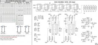
I'm trying to put together a new Miro AD1862 dac using Patrick's CEN IV stage. I'll be using an older JLS USB to I2S to feed it. I want to keep some flexibility with front ends for the dac so I installed the shift registers and plan to feed them from the normal I2S outs on the JLS board. So the first task for me is to get the dac functioning using the existing opamp IV stage, after which I will remove the Riv and Civ from the dac board and attempt to hook up the Cen IV. My eyes aren't what they used to be, and in my haste to assemble the dac I discovered two screwups when doing voltage checks, C7 was reversed and IC4 was installed upside down. I have corrected both issues and taken a new voltage data set. Before risking my precious Dac chips do any of you more seasoned builders see anything wrong with these readings. I appreciate any input.
I'm trying to put together a new Miro AD1862 dac using Patrick's CEN IV stage. I'll be using an older JLS USB to I2S to feed it. I want to keep some flexibility with front ends for the dac so I installed the shift registers and plan to feed them from the normal I2S outs on the JLS board. So the first task for me is to get the dac functioning using the existing opamp IV stage, after which I will remove the Riv and Civ from the dac board and attempt to hook up the Cen IV. My eyes aren't what they used to be, and in my haste to assemble the dac I discovered two screwups when doing voltage checks, C7 was reversed and IC4 was installed upside down. I have corrected both issues and taken a new voltage data set. Before risking my precious Dac chips do any of you more seasoned builders see anything wrong with these readings. I appreciate any input.
Attachments
Hi Fran,
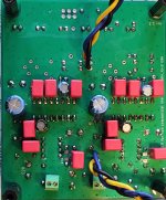
Yes this it the pic before I found I had reversed IC4, used this pic magnified to find that out. I'll try reflowing the shift register pins and check again with another DMM. I had fresh batteries in this one but it seemed to be acting a bit strange.
Iggy,
I am no expert on the sound of capacitors these were available to me and seemed to be good quality modern caps. Do you have any suggestions for a better choice ?
Sat on these boards for well over a year now and you can tell because it's an outdated layout but it still works! Soldering small pads with small relief area but needing a big tip with lots of heat for such a big GND plane created some drama where I had a solder bridge on the +5V rail because I just slightly nicked the solder mask around J7 (back side) on the GND plane and ended up removing every component on the +5 net before I figured out it was a very, very small bridge.
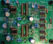
Happy to say I've successfully built my first diy dac so the next build shouldn't be nearly as scary. Does this get me into the AD1862 club now?")
Dont mind the KA caps, they were in the drawer and this was only to see if I could figure out the BOM mystery. Seeing all these other builds with 1/2 the components not installed was very confusing.
Cheers!
Stephen


Happy to say I've successfully built my first diy dac so the next build shouldn't be nearly as scary. Does this get me into the AD1862 club now?
Dont mind the KA caps, they were in the drawer and this was only to see if I could figure out the BOM mystery. Seeing all these other builds with 1/2 the components not installed was very confusing.
Cheers!
Stephen
but I found it was very slow to come up to voltage.
That would be fatal for the SMD FC CEN IV.
So don't use anything that takes seconds to come up to voltage.
Patrick
Yes, it's the VRDN. I can only use it on the 12V side because you can't get it down to 5V so that is coming from a bench supply off camera.
I had the VRDN on the bench meter to adjust it to +/-12V and although I don't remember it being slow to come up, it does definitely bounce back and forth for about half a minute before stabilizing at the target voltages. For example, at 12V, it overshoots by about 0.5V if I remember correctly and then undershoots by a bit less than that and then goes back to overshooting ... it does this maybe 6-8 times, getting closer to target each time before it stops bouncing.
Noted about the CEN I/V though and will definitely not use it for CEN testing.
On another note, I have a Twisted Pear Buffalo (ESS9008) that I've been sitting on for close to 15 years and now that the dac fog is lifting, I found a manual and got it connected and running for the first time! The difference being that I have an XMOS module to provide I2S as I couldn't understand how to connect SPDIF to the Buffalo. Small victories!
You may wish to explore other caps eventually but I used these caps on one of my AD1862 boards. I have not found them to be offensive so far.Dont mind the KA caps, they were in the drawer and this was only to see if I could figure out the BOM mystery. Seeing all these other builds with 1/2 the components not installed was very confusing.
Dont mind the KA caps, they were in the drawer and this was only to see if I could figure out the BOM mystery. Seeing all these other builds with 1/2 the components not installed was very confusing.
Cheers!
Stephen
It is ok where you put them on the photograph, i.e. only on the 5V side... I would avoid the RN55 resistor (the brown ones) on the analog and I/V role though.
This test was deliberately pumping excessive power into the resistors to make distortion measurable :
https://convexoptimization.com/TOOLS/SimonVishay.pdf
This is what Mr. Hofer (Audio Precision) had to say :
https://hifisonix.com/wp-content/uploads/2017/11/Designing_for_Ultra-Low_THD_N-1.pdf
But of course some people prefer to hear distortions on purpose and worship carbon resistors, etc.
That is another story.
Patrick
A 2.7k RN55 25ppm driven at full scale current in a sine wave by the AD1862 has a temperature rise of 0.19 degC.
Or a resistor change of 5ppm, of which only a small portion contributes to H3.
That would be in the order of <-110dB.
But of course you rarely have full scale output continuously from a DAC.
I cannot hear distortion this low, as it would be masked by my Speakers anyhow.
Of course if you have high current-out DACs, that is another matter.
Patrick
well I would say this is something else as it is clearly in the musical playback. I really do not like this RN55. But I do not encorage people to remove them from their board as the risk of wasting active parts with the heat, layout of the board (vias), etc is not worthing the hassle.
- Home
- Source & Line
- Digital Line Level
- DAC AD1862: Almost THT, I2S input, NOS, R-2R