No worries!
I was talking about C3, C4, (the ones that keep it from oscillating to death) on the mosfet boards. Always use. I will go back and edit that into my post for clarity.
C1, C2, on the FE board are just local PSU decoupling. So are C1x C2x.
I was talking about C3, C4, (the ones that keep it from oscillating to death) on the mosfet boards. Always use. I will go back and edit that into my post for clarity.
C1, C2, on the FE board are just local PSU decoupling. So are C1x C2x.
Last edited:
Actually my question relates to the c1x/c2x on the output boards. I see the caps on the fe board and on schematic and those make sense to me.it’s the ones on output boards that I simply cannot find on v3 schematic. I’ll look again. So for a 4pr device v3 monoblock, (2 n boards on one sink and 2 p boards on other sink), I should populate c1x and c2x on only one of the n boards and one of the p boards? Does it matter which board, ie, closer to fe or daisy chained one? Thank you both for helping me understand. Happy and healthy new year to all.
also, what cap value are c1x and c2x? i thought the 1000pf c3 and c4 were the anti-oscillation caps. thx
Thank you!
I am having a fit posting pics, but let me see if this will work.
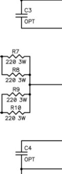
I thought (unless I am using the wrong schematic, so please forgive me) that C3 and C4 in the snip of the schematic below were for the oscillation. Listed as optional, but strongly recommended.

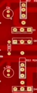
C3 and C4 are (I think) in line with the center of the N and P boards close to the TPs. I just can't see well enough on the pic to post it, nor do I have a board to trace.
C1 and C2 (as noted on the schematic in the first post and on the V3 boards) are here... along with their neighbors C5 and C6.

C1x and C2x are on the N and P boards here.

Everything for everyone, should be prefaced with a big ol' fat, I think. B/C I am not near a set of boards and don't have a decent display to work with at the moment.
Perhaps, @algg could post some pics that are much better than my attempted grabs.
Thanks!!!!
Edited to add - They've just posted, so perhaps it will be easy-peasy for you two to chat back and forth. I'd love to understand the outcome.
I am having a fit posting pics, but let me see if this will work.
I thought (unless I am using the wrong schematic, so please forgive me) that C3 and C4 in the snip of the schematic below were for the oscillation. Listed as optional, but strongly recommended.

C3 and C4 are (I think) in line with the center of the N and P boards close to the TPs. I just can't see well enough on the pic to post it, nor do I have a board to trace.
C1 and C2 (as noted on the schematic in the first post and on the V3 boards) are here... along with their neighbors C5 and C6.

C1x and C2x are on the N and P boards here.

Everything for everyone, should be prefaced with a big ol' fat, I think. B/C I am not near a set of boards and don't have a decent display to work with at the moment.
Perhaps, @algg could post some pics that are much better than my attempted grabs.
Thanks!!!!
Edited to add - They've just posted, so perhaps it will be easy-peasy for you two to chat back and forth. I'd love to understand the outcome.
Oh jeebuz, I really need to look things up before posting… My apologies…
On the Mosfet boards, the anti-oscillation caps are C3, C4. Always use.
C1x and C2x are repeats of C1 and C2. Look at the schematic, they are electrically in the same position as C1 and C2, but since the PCB is split into 3+ pieces, they are repeated on the mosfet boards. In my opinion C1x C2x are not needed, since they are on the mosfet boards, and C1 C2, on the front end board, is where they should be.
Last edited:
That's what I had thought, but really needed confirmation on. I could not see the back of the board in any pics to confirm if C1x and C2x were going to be electrically identical to C1 and C2. Also, thank you for the note of preference for placing them on the FE boards. Into the notes that thought goes.
Sorry for causing any confusion @algg! With the board revisions, I just could not be sure, and I should have waited for someone else to answer initially.
Thanks!!!!
Sorry for causing any confusion @algg! With the board revisions, I just could not be sure, and I should have waited for someone else to answer initially.
Thanks!!!!
Lol!! I love you guys! I chuckled when I scrolled down and saw the post-it notes on pcbs. Now you are talking at my level. Everything is very clear and i can’t thank you both enough. Can’t wait to start building. Thought I could get started over the holidays but dontcha know, holidays never work out the way you plan. Best,
At some point I did want to try putting the diodes back in the circuit. I've never built with them, but I saw some promise in using Higher Vf diodes with a bias point and source resistors set to not allow conduction until about 4A of current. The trouble is, not many speakers will draw that much current at sane listening levels.
Of all the amps I built since the F5T was published (over ten years ago now), three amps were built with laterals in the output (obviously configured differently - no thermistors, no current limiting, no feedback cap and 15dB gain), other four with verticals. These are the issues I faced:
The first one I built came back after three years for suspected output device failure (smoke emission) but it was fine, no issues except for a slightly browned CRC resistor in the power supply. I actually left it in there, so that it would be the first to die in case something did go wrong.
Another one - this one is seven years old - is sitting on my desk with bias runaway on one channel, with suspected trimmer failure (the one time I decided to trust a Vishay trimmer instead of Bourns). It is testing fine after replacing the trimmers and only the trimmers. I don't have a green light on the power supply, which I'll get to next.
One had locally sourced MUR860s in the power supply which turned out to be fake, and it took out the transformer. Amp and speakers were both fine, and replacing the power supply was all that was needed.
The PCB in use for most builds was a single 300mm wide board for the whole circuit, three pairs of outputs - and I always used all three. V-grade devices for verticals, BL for laterals. Always used the cascode, usually 2SB669/D649 pair. JFET and cascode both had heatsinks - this is a hot country. JFETs set to run in 8-10 volt range, rather than half-supply.
The PCBs were ordered in one lot of 10 from JLC, and the layout permits downsizing the 1nF feedback caps to 220pF. The thermistor arrangement is taken from the older Tea-Bag version (thermistor + resistor between gate and output instead of one device drain), with a small cap across the thermistor that further enhances stability and bypasses it at HF. We get pretty poor quality parts in India, so have to make these modifications to suit them.
I only used the V1 circuit with these personal alterations. FWIW. I'm no longer building these - just too heavy for me, but it was a fun journey and it's taught me more than I ever thought I'd know. All due to Nelson's generosity in sharing his creations with us.
Are the MUR3020WTG from Onsemi the best choice, or the Vishay VS-MUR3020WT-N3?The “turbo” effect is depending on the temp coefficient of the MUR3020 specifically.
If one decides to use the diodes... Thanks!
Well, there are not enough of the Vishay in stock, so it’s kind of a moot question… 
Either should work fine.

Either should work fine.
Are you not using a standard chassis with big heatsinks?
Edited to add - In some schematics those are an output pair. Too many schematics and designations. You posted clarification after I had posted. I like these, but there are a bunch of options.
https://www.mouser.com/ProductDetail/532-551002B00G
Edited to add - In some schematics those are an output pair. Too many schematics and designations. You posted clarification after I had posted. I like these, but there are a bunch of options.
https://www.mouser.com/ProductDetail/532-551002B00G
Member chuckd wrote a wonderful bias procedure, here it is so it's easy to reference. 🙂
````````
Bias Procedure for F5 Turbo Version 2
After you have completed your build you need to bias the output (measured in mV) in order to generate enough power to activate the MOSFETS. You need to do this while keeping the DC Offset (the potential across the speaker terminals) at 0V. This is achieved by increasing gradually, in an alternating pattern, the resistance of P1 and P2. You are not directly measuring the resistance but the voltage across P1 and P2.
Things you’ll need:
3 x DMM
1x Variac
1 x completed F5 Turbo v2
Set P1 and P2 to 0Ω
Setting these to 0 prevents current flow through the FE stage while you power up the amplifier. To make sure you are starting at zero bias at the beginning.
- Attach leads to TP1 and TP2, and TP3 and TP4 on the front end board.
- Turn P1 and P2 whichever way is required to set the resistance across the test points to 0.
- Make an arrow on each pot to indicate what way to turn the pot to increase resistance. Clockwise may not be “up”.
Powerup the amp, check the PSU voltages.
- Make sure the Variac and the power entry module (PEM) (the Schurter switch) are correctly and properly fused.
- Connect the PEM to a Variac or light bulb tester with appropriately current rated power cord (AWG12 and above should suffice).
- Turn Variac to 0V.
- Switch Variac and amp on.
- Check voltage between positive and negative (neutral in the U.S.) with the DMM (set to check VAC) across the barrier block connection. Ensure it reads 0V.
- With the leads still connected to the terminals, slowly increase the voltage on the Variac. If smoke appears turn off the power and troubleshoot the problem. If the fuse blows, the there is a short in the system. Locate and troubleshoot the problem.
- If there is no smoke, continue slowly increasing until you reach mains voltage.
- Once at mains voltage, you can check the step down AV voltage across the secondaries to ensure it matches the value of the transformer.
- Switch DMM to measure DC volts.
- Check the voltage out of the rectifier and before the capacitor bank to ensure it is DC.
- Finally, check the DC voltage at the terminals of the PSU. This is the power that will go to the Gain Stage and Output boards.
- Connect the positive lead of the DMM to the V+ and the negative lead to GND. You should have a positive reading.
- Now connect the positive lead from the DMM to GND and the negative to V-. You should have the same potential but a negative signal.
- If you don’t you need to check your wiring.
- If you do then proceed to setting the bias.
Setting the bias
- Make sure the mains are at max voltage. Remove a light bulb tester if you are using one.
- Set your three DMMs to check DC voltage. If the DMM is manual, set to 2V or 20V.
- Using alligator clips, attach one DMM to TP2 and TP3 on the output boards: One on the P-Channel and one on the N-Channel. Ensure it reads 0V. These will measure the bias.
- Attach the third DMM across the speaker output. Ensure it reads 0V. This will measure the DC offset.
- Grab an insulated screw driver and turn P1 (or P2 – it doesn’t matter) 360o. There may be no change on the DMM. This is normal.
- Turn the other potentiometer 360o. Again, there may be no change in the voltage. This is normal.
- Continue alternating increasing P1 and P2 with 360o turns until you start to read a voltage across the potentiometers.
- While increasing the resistance, keep a watch on the DC offset. It will increase or decrease depending on which potentiometers you turn. It should remain around 0V.
- Continue alternating turning P1 and P2 and bring them up to 300 mV (0.3V). Ensure that the DC offset remains at 0V.
- As you get closer to 300mV, you may have to adjust the turns to a smaller amount since a full turn can have a dramatic change in voltage.
- The heat sinks should be warming up.
- Once you get the bias on each output board to around 300mV (there may be a slight difference in order to keep the DC offset at 0V. It is ok if the bias voltage difference is within 50mV, and the offset zeroed.
- Set the lid on and let the amp rest (or ‘cook’) for 20 minutes.
- Keep a watch on the DMMs. As the thermistors heat up they will adjust to keep the DC offset at 0V.
- The bias may change as the MOSFETs heat up. This is normal and should settle after about 20 minutes.
- After 20 minutes, and if the bias readings have settled, and there is no smoke, increase the bias to 350mV by alternating turning P1 and P2.
- You may not get exactly 350mV bias on both boards at the same time as keeping the DC offset at 0V. This is normal. Get the bias between P1 and P2 as close as you can to each other within the 350mV range all the while with DC offset at 0V.
- Let the amp cook for another 20 minutes.
- The bias should not change too much, if at all, since the heat sinks have already warmed up.
- If this is a stereo amp, repeat this process for the other channel.
- Once the other channel is done, recheck the bias and DC offset for the first channel, and make any adjustments to the bias to bring it up/down to around 350mV and 0V DC offset.
- That’s it! Congratulations, you have just biased your amp.
- Turn off the amp and let it cool a little.
- Attach your test speakers (if you have them) and turn on the power. If nothing happens then you should be able to integrate the amplifier to your system.
- If you don’t have test speakers, and you attach them to your system speakers, you run the risk of damaging them. So proceed down this path at your own risk.
hello, new bee here with a question? i have a problem with not able to get enough bias on my newly build f5 turbo. i was able to get 250mv but for some reason i ran out of adjustment. any help would be appreciated.
give details aboyt JFets are using (rang, measured Idss) and point us to reference schematic
pretty much - all you need is to increase resistors in parallel to trimpots in drains of input JFets
pretty much - all you need is to increase resistors in parallel to trimpots in drains of input JFets
my jfets were purchased from the diy audio storeMatched JFETs - Toshiba 2SK170/2SJ74 Quad 6-8mAgive details aboyt JFets are using (rang, measured Idss) and point us to reference schematic
pretty much - all you need is to increase resistors in parallel to trimpots in drains of input JFets
- Home
- Amplifiers
- Pass Labs
- F5Turbo Illustrated Build Guide