Nothing wrong with the schematic, better than 99,99% forum's designs, it's just that they didn't know at that time where sound quality was lost. Not to mention that's even more sad that still in these days folks don't have a clue.")
And you are that 0.01%, all the rests don't have a clue.
I believe, what LC means, is related to overall build quality. For example, some of the amplifiers surprised me with their small PSUs and thin wires at that time.
Example of the good build approach for me - Accuphase M-60. Single channel monoblock weights 27 kilos. They still sound great, if you can find them
Another good example - Sony TA-NR1 with its virtually unlimited output current capability. Also very heavy one.
Example of the good build approach for me - Accuphase M-60. Single channel monoblock weights 27 kilos. They still sound great, if you can find them
Another good example - Sony TA-NR1 with its virtually unlimited output current capability. Also very heavy one.
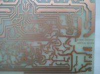
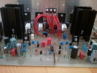
Cool DIY-friendly build on a single-sided PCB!
Guys, here is a great work by George (member filenet).
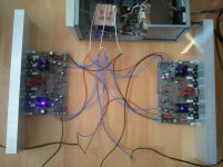
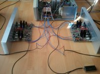
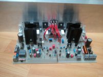
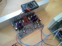
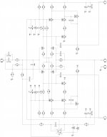
He has re-designed the PCB, combining the VERTICAL front-end and NS-OPS with 2SC5200/2SA1943 output devices, and making is easy to etch.
George allowed me to publish his photos, I also take the liberty to show a fragment of his message, so that you see the key amendments he did as well as his impressions:
I finished your Vertical NS-OPS. I made some `slight` modifications to it:
1. I am using +/-60v power supply with only 20000uF per rail from an old project.
2. I changed the output devices to 2SC5200/2SA1943. Also here i am using a zobel network and a big inductor with 10ohm resistor.
3. I changed R1 2k7 resistor with 4k7.
4. I changed 22uF capacitors to 47uF because this is what i had in stock.
5. The boards are THT single layer (see the pictures).
I must admit i was a little anxious when i first switch the power on, about everything turning into a 200w oscillator. That never happened.
The amplifier is stable. It has little hum when the inputs are not connected to a source, that`s ok , i do not intend to use the amp not connected to anything.
The sound is top class without the huge class A dissipation
Now such an amp deserves a 21 century protection.
Congratulations George for your successful build and thanks for sharing your experience. The design becomes really mature
You inspire me to come up with my version of the layout, combining both Vertical and NS-OPS on one board, having all the outputs on one side
Cheers,
Valery
Guys, here is a great work by George (member filenet).
He has re-designed the PCB, combining the VERTICAL front-end and NS-OPS with 2SC5200/2SA1943 output devices, and making is easy to etch.
George allowed me to publish his photos, I also take the liberty to show a fragment of his message, so that you see the key amendments he did as well as his impressions:
I finished your Vertical NS-OPS. I made some `slight` modifications to it:
1. I am using +/-60v power supply with only 20000uF per rail from an old project.
2. I changed the output devices to 2SC5200/2SA1943. Also here i am using a zobel network and a big inductor with 10ohm resistor.
3. I changed R1 2k7 resistor with 4k7.
4. I changed 22uF capacitors to 47uF because this is what i had in stock.
5. The boards are THT single layer (see the pictures).
I must admit i was a little anxious when i first switch the power on, about everything turning into a 200w oscillator. That never happened
.The amplifier is stable. It has little hum when the inputs are not connected to a source, that`s ok , i do not intend to use the amp not connected to anything
.The sound is top class without the huge class A dissipation
Now such an amp deserves a 21 century protection.
Congratulations George for your successful build and thanks for sharing your experience. The design becomes really mature
You inspire me to come up with my version of the layout, combining both Vertical and NS-OPS on one board, having all the outputs on one side
Cheers,
Valery
Attachments
-
 2016-02-06 13.04.52.jpg157.2 KB · Views: 728
 -
 2016-02-09 15.31.35.jpg174 KB · Views: 298
 -
 2016-02-09 15.28.08.jpg202 KB · Views: 372
 -
 2016-02-09 12.05.58.jpg159.8 KB · Views: 681
 -
 2016-02-09 12.04.50.jpg157.3 KB · Views: 691
 -
 2016-02-09 12.02.13.jpg186.6 KB · Views: 687
 -
 2016-02-09 11.49.32.jpg155.6 KB · Views: 712
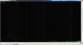
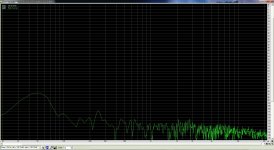
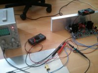
I made screenshots on maximum noise level.
(closed input and open input)
What amp is this?
What amp is this?
All so bad?..

(Instead listening noise in loudspeaker better to look it on spectrum).

All so bad?..
(Instead listening noise in loudspeaker better to look it on spectrum).
No, I'm just curious, what amplifier were those spectrums taken from?
Guys, here is a great work by George (member filenet).
He has re-designed the PCB, combining the VERTICAL front-end and NS-OPS with 2SC5200/2SA1943 output devices, and making is easy to etch.
George allowed me to publish his photos, I also take the liberty to show a fragment of his message, so that you see the key amendments he did as well as his impressions:
I finished your Vertical NS-OPS. I made some `slight` modifications to it:
1. I am using +/-60v power supply with only 20000uF per rail from an old project.
2. I changed the output devices to 2SC5200/2SA1943. Also here i am using a zobel network and a big inductor with 10ohm resistor.
3. I changed R1 2k7 resistor with 4k7.
4. I changed 22uF capacitors to 47uF because this is what i had in stock.
5. The boards are THT single layer (see the pictures).
I must admit i was a little anxious when i first switch the power on, about everything turning into a 200w oscillator. That never happened
The amplifier is stable. It has little hum when the inputs are not connected to a source, that`s ok , i do not intend to use the amp not connected to anything
The sound is top class without the huge class A dissipation
Now such an amp deserves a 21 century protection.
Congratulations George for your successful build and thanks for sharing your experience. The design becomes really mature
You inspire me to come up with my version of the layout, combining both Vertical and NS-OPS on one board, having all the outputs on one side
Cheers,
Valery
I started doing a version like this, but didn't get far. I'm looking forward to your results! ( Hint, An extra MJE340 and a 4 pin header to match the 21st century board is a welcome option).
Last edited:
I started doing a version like this, but didn't get far. I'm looking forward to your results! ( Hint, An extra MJE340 and a 4 pin header to match the 21st century board is a welcome option).
What do you mean by an extra MJE340?
What do you mean by an extra MJE340?
Temperature sensing for the control board. Less external parts are nice. I've made the amplifier connections on the control board a single 4 pin header to each amplifier channel.
Pin 1- Bias +
Pin 2 - Bias -
Pin 3- temp
Pin 4- ground
A simple 4 wire ribbon to each amplifier would clean up installation.
Ah, I see. Integrated temp sensor - that's good
I'm curious where the open circuit noise is coming from. I haven't had time to experiment yet. Would the addition of Shuntie to the input board supply help?
I don't think it's coming from the rails - in this case it would stay with the input connected to the pre-amp. Also, the input stage is additionally filtered with zeners and RC. So, I don't think the Shunties will really help. Although, the effect is interesting and I'm also going to work more on it.
I have designed a VFA option of VERTICAL - that one has got a better PSRR by design, as well as lifted ground option, being in the same league in terms of overall speed and distortion. So, we'll see.
This is going to be a real CFA vs VFA rumble
Attachments
I'm just placing a stock order here. It's looking like 2n5401 is extinct from On Semi and Fairchild and has become an expensive part.
Hmm... 2n5551/5401 have always been the high-enough-voltage-nothing-special-general-purpose transistors. Surprise
I will probably also refill some stock here then - thank you for the info
Hello
I have some general question. I am drawing a new simple OPS board now with 3 pairs of BJTs.
I have room on the board to fitt 16mm diameter electrolitic capacitor next to each of the collectors of OP transistor. The biggest capactance I can get in 16mm diameter is 1000uF.
Now the question is if decoupling amount of 1000uF for each transistor isnt too much.
The ground return will be separate for OPS and IPS boards.
Big Thanks.
Peter
Hello
I have some general question. I am drawing a new simple OPS board now with 3 pairs of BJTs.
I have room on the board to fitt 16mm diameter electrolitic capacitor next to each of the collectors of OP transistor. The biggest capactance I can get in 16mm diameter is 1000uF.
Now the question is if decoupling amount of 1000uF for each transistor isnt too much.
The ground return will be separate for OPS and IPS boards.
Big Thanks.
Peter
Hi Peter,
Good question. Normally, both Ostripper and myself, are using much smaller values for local decoupling - 22uF is enough. I would say, up to 100uF is a practical maximum. You've got the big main filtering arrays anyway, plus hopefully some local decoupling on the power amp board, close to the power terminals (470-1000uF is a good value there). So, the ones, close to each transistor, are just an addition to all that, filtering local ripple... don't have to be that big.
Cheers,
Valery
- Home
- Amplifiers
- Solid State
- Revisiting some "old" ideas from 1970's - IPS, OPS