Not yet but I was curious to look at class A CFP. I haven't seen many others.Correct. Did you build the kit?
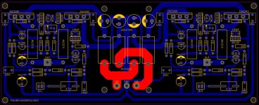
OK I am attaching the top overlay of the pcb the resistors in parallel with the fuse holders are 100R 5W for safe set up purposes without fuses in the voltage rail holders. This strategy has been used in numerous amplifier projects published in Australian Electronics magazines going back at least to the mid 1970's when I built a "Twin 40 Playmaster amplifier - my second power amplifier project. The only trouble I had with this was fitting the wrong value of resistor in the preamp section. The telling multiplier band colour was hard to determine. The second attachment shows the copper pattern. I am not trying to divert attention from the P3A in posting these images but with the thought they might inspire/help Sadface in his objective to design a new pcb for his P3A.
Attachments

One thing you will see is that sticks out is the location of the Vbe transistor free standing with small air gap between this and a reflection of the front face of that transistor on the heat sink shiny side. Since Class A amps run hot this is understandable however there is a large heat sink for P3A where the Vbe transistor is tied to a driver if so why is there a need for such a large heat sink?
Last edited:
I'm playing with the p3a too, an intriguing little amp, with great potential, I will just say, don't forget about the power supply, in my experience with p3a it shines with a brute force crc or similar, intended for class A , even though only AB.
I've tried with crc today and will also try chokes.
Ps nice boards sadface I like the 10r ground and degen resistors, a group buy in future?
Pps nearly wetted my pants earlier, a ground crocodile clip hit the plus bus bar, jesus, 150000uf discharge

I've tried with crc today and will also try chokes.
Ps nice boards sadface I like the 10r ground and degen resistors, a group buy in future?
Pps nearly wetted my pants earlier, a ground crocodile clip hit the plus bus bar, jesus, 150000uf discharge
Interesting the way that the power rails are separated before the fuse so the fuse only goes to the outputs, I've not seen anything like that before.OK I am attaching the top overlay of the pcb the resistors in parallel with the fuse holders are 100R 5W for safe set up purposes without fuses in the voltage rail holders. This strategy has been used in numerous amplifier projects published in Australian Electronics magazines going back at least to the mid 1970's when I built a "Twin 40 Playmaster amplifier - my second power amplifier project. The only trouble I had with this was fitting the wrong value of resistor in the preamp section. The telling multiplier band colour was hard to determine. The second attachment shows the copper pattern. I am not trying to divert attention from the P3A in posting these images but with the thought they might inspire/help Sadface in his objective to design a new pcb for his P3A.
It makes sense since there shouldnt be multiple amps going anywhere else.
The grounding layout looks very similar to mine: power ground around the outside and signal grounds all collecting at the central GND connection.
Is the relevant detail here the central high current ground trace?
It does follow the idea of connecting the positive and negative before connecting to the star.
It is better to think in terms of transconductance (gm) = Ice/Vbe which is measured in Siemens (S) where Ice is 1Amp and V is 1Volt. That can be scaled down to m.a./mv = mS for rough calculations small signal transistor gm in mS is in the vicinity of 40 times the bias current. A small adjustment m.v. is enough to increase bias current to cover any likely need at the level amplifiers work at. Av=gm in mS by RL in k Ohms for signal frequencies so the load presented to the Vas by the output stage is a relevant factor. That is a reason why EF3 designs exist.Is a higher hFE rating or a lower hFE rating preferable for Q4/Q5/Q6?
Last edited:
You could have been more worried if that was a river crocodile. It may be time to avoid accidents for you think about putting this in a caseI'm playing with the p3a too, an intriguing little amp, with great potential, I will just say, don't forget about the power supply, in my experience with p3a it shines with a brute force crc or similar, intended for class A , even though only AB.
I've tried with crc today and will also try chokes.
Ps nice boards sadface I like the 10r ground and degen resistors, a group buy in future?
Pps nearly wetted my pants earlier, a ground crocodile clip hit the plus bus bar, jesus, 150000uf discharge View attachment 1220266
Happy it was a small metal one that snapped at me, I'm no steve irwin, chassis is ready but still trying out various power supplies, until now the crc with 47000uf after rectifier then 1 ohm and 100000uf is not bad.
Yes I know its overkill, but had them already.
Will try a pair of chokes later, instead of resistors, 15mh dc resistance 0.2.
Also pulled out the wima 4.7uf input cap and replaced it with a Russian type k73-16 1uf 400v, sound stage feels deeper.
Lots of fiddling to do..
Yes I know its overkill, but had them already.
Will try a pair of chokes later, instead of resistors, 15mh dc resistance 0.2.
Also pulled out the wima 4.7uf input cap and replaced it with a Russian type k73-16 1uf 400v, sound stage feels deeper.
Lots of fiddling to do..
One of the advantages (perhaps the only?) of a CFP design is that the quiescent current can be held remarkably constant because of the local feedback which excludes the Vbe of the output pair.
For this to work well, the drivers and bias regulator need to be mounted on a small heatsink together. That means insulating the heatsink, of course, and using a BD139 for the bias regulator which can be easily mounted with its mounting hole.
It is also better to keep the drivers running cool and putting small heatsinks on them. In the past I have mounted the bias regulator underneath one with one of the drivers on top. The heatsinks are small 20x20x20mm finned types. The insulator was between the bias stabiliser and heatsink so that the driver had direct thermal contact as did the other driver.
Did anyone mention this?
Regarding stability, small emitter resistors in the driver will help to reduce the gain in the CFP feeback loop, but I would suggest using the lower frequency MJL21193/4 would be a better choice if the higher frequency devices still give trouble.
I think a better stability configuration would be possible but it would need some simulation to sort out.
Degenerating the input stage will help but DC offset is still an issue if the currents are not matched. A current mirror in the collectors would help - but may impact stability - each transistor added adds a free additional frequency roll-off which may (usually) makes things slightly worse. For that reason alone, I am actually tempted to say keep the resistor loading but ensure that the currents in the diff pair are as equal as possible. Distortion cancellation requires that. This can be achieved by careful selection of the current source LED and emitter resistor. I'd be tempted to use a 5.6 Zener and higher resistor value instead, perhaps with a pot. to adjust the current.
I have posted an amended circuit for the P3a on a current thread Linearising the CFP crossover P3a.
It was convenient to do a simulation on that thread as there was an .asc attachment I could use and adapt to return a favour for the trouble taken by the member who drafted the original circuit.
I had to make some marked changes in some resistor values from those that Rod Elliott used, and checked these progressively as I went. I started with resistors in the bootstrap circuit. In previous iterations for P3 the predecessor versions these were 2k2 compared to 3k3 for P3A.
These did not look right.
Initially there were zigzag patterns on sine wave with capacitive loads - see the second image included in post 1 for 1kHz signal input.
If there are LTSpice users some might look at my circuit and use the .set param command to test a range of values in a single test series operation to find the best results. As things stand the zig zag pattern on 20kHz should not be in evidence.
OK,
I think I have managed to keep the extra rail decoupling and fix the grounding.


The input cap was changed to 13mm width to fit a Wima MKP4 4.7uF
R13/R14 changed to be 3x 2W 1R carbon film resistors.
I also added the extra pads to solder in the safety resistors over the fuses as I really like that idea.
I think I have managed to keep the extra rail decoupling and fix the grounding.
The input cap was changed to 13mm width to fit a Wima MKP4 4.7uF
R13/R14 changed to be 3x 2W 1R carbon film resistors.
I also added the extra pads to solder in the safety resistors over the fuses as I really like that idea.
I largely agree that mjona has the right solution to the problem. (refer to his circuit in Linearising the CFP crossover P3a).
The points I would make are firstly that I think the VAS current is too low and I would have chosen a higher current.
The Miller capacitor configuration in the original p3a is not optimum and although I have not investigated whether this is the cause of a triangular 20kHz as mjona says, it certainly has the capability of doing that.
The approach mjona has shown was also that I have recommended and first suggested by Dr Bailey. It surprises me that the Miller approach still seems to permeate the airwaves on here, though when using more stages it usually requires more careful compensation.
The other suggestion, I repeat, is to make the bias stabiliser a BD139 also, and mount the stabiliser and driver transistors on a small shared heatsink, separate to the output device heatsink.
None of these ideas are new - the idea of thermally coupling the drivers/bias in a CFP design was in Practical Electronics in the early 1970's using Zetex devices and MJE3055/2955 outputs.
The features which Bailey used were phase lead compensation as mjona shows, and "sprog" suppressing resistors in series with the driver bases.
For what it is worth, John Linsley Hood also favoured the phase lead compensation, in the main.
It is possible to use the phase lead compensation with an emitter follower /current mirror stage before the VAS (as in the Blameless) but it takes a little more to control.
If folk want to use the Miller scheme, I would advocate increasing the current in the input differential pair with sufficient degeneration to prevent overloading with high frequency signals, as demonstrated by Stochino. (The current does not have to be as high as 10mA though).
The features which Bailey used were phase lead compensation as mjona shows, and "sprog" suppressing resistors in series with the driver bases.
Can you elaborate on the "Sprog" resistors? It sounds like you are referring to what is typically described as base stoppers. I've searched this forum and google and the only references to "sprog" I found comes from posts your have made on these forums.
"sprog" was a term used by colleagues who were into radio comms when I was a student. It derives from "spurious oscillation" in a radio receiver (or transmitter).
When a resistor is in series with a base lead it reduces the frequency response, and Bailey used that effectively to make his phase lead compensation work. Also used as gate stoppers in MOSFET circuits. Those really are "sprog" stoppers as they don't "stop the gate" but parasitic oscillations.
Ed Cherry also used the term "sprog stoppers" in his article on nested feedback in ETI, another old electronics mag in the UK.
It could of course have derived from unwanted "offspring" in a circuit ....
- Home
- Amplifiers
- Solid State
- Stability testing my new Rod Elliot P3A