
I figured out how to get the driver stage decoupling ground trace from the positive rail to the star separate from the output stage ground trace.

However I can't figure out how to resolve the negative rail with the positive rail separate from the star.
The best I can come up with is to use a jumper like this:

This would allow me to resolve positive and negative grounds from the various decoupling stages separate from each other and still keep all the signal grounds separate too.
I have also indicated in yellow where I will place a heatsink across the 2 drivers. My plan would be to cut some 2mm aluminium with a cutout to go over the top of R13/R14 so that the 2 drivers are on the same heatsink. My plan would also be to drill some holes to either side of Q6 so that a cable tie can still be used to thermally couple Q9 to Q6 as Rod recommends.
The other option would be to do as John Ellis suggests and use a BD139 for Q9 with some flying leads so that it could be bolted directly to the driver heatsink. Or plausibly with a lot of rework on the layout, Q9 and the trimpot could be mounted in between R13/R14 so that it is mounted in the centre of the driver heatsink; equidistant from the 2 drivers.
Oh I also added an extra hole on the ground trace at the bottom as an easily accessible test point. I figure that the holes added for the safety resistors on the fuse rails serve the same purpose as test points.
However I can't figure out how to resolve the negative rail with the positive rail separate from the star.
The best I can come up with is to use a jumper like this:
This would allow me to resolve positive and negative grounds from the various decoupling stages separate from each other and still keep all the signal grounds separate too.
I have also indicated in yellow where I will place a heatsink across the 2 drivers. My plan would be to cut some 2mm aluminium with a cutout to go over the top of R13/R14 so that the 2 drivers are on the same heatsink. My plan would also be to drill some holes to either side of Q6 so that a cable tie can still be used to thermally couple Q9 to Q6 as Rod recommends.
The other option would be to do as John Ellis suggests and use a BD139 for Q9 with some flying leads so that it could be bolted directly to the driver heatsink. Or plausibly with a lot of rework on the layout, Q9 and the trimpot could be mounted in between R13/R14 so that it is mounted in the centre of the driver heatsink; equidistant from the 2 drivers.
Oh I also added an extra hole on the ground trace at the bottom as an easily accessible test point. I figure that the holes added for the safety resistors on the fuse rails serve the same purpose as test points.
Hugh,
Thanks for that. Some time ago I tried to contact Ed through the university but could not find any contact details, so assumed he had retired.
His nested feedback idea was quite novel in audio design. I have found that the major improvement in his design for reducing crossover distortion seemed to be the use of inclusive Miller compensation, and he well understood the idea of using degen in the input stages to prevent slew rate overloading, which Stochino later exploited.
Sorry to hear that he is suffering, cancer is not nice.
Not recommended. You want the junction of the bias transistor as close as possible to the drivers junction to thermally track it with as little thermal lag as possible.Or plausibly with a lot of rework on the layout, Q9 and the trimpot could be mounted in between R13/R14 so that it is mounted in the centre of the driver heatsink; equidistant from the 2 drivers.
I have revisted the simulation I posted on the other thread about linearising the P3a. I did not look at changesto the LTP.One of the advantages (perhaps the only?) of a CFP design is that the quiescent current can be held remarkably constant because of the local feedback which excludes the Vbe of the output pair.
For this to work well, the drivers and bias regulator need to be mounted on a small heatsink together. That means insulating the heatsink, of course, and using a BD139 for the bias regulator which can be easily mounted with its mounting hole.
It is also better to keep the drivers running cool and putting small heatsinks on them. In the past I have mounted the bias regulator underneath one with one of the drivers on top. The heatsinks are small 20x20x20mm finned types. The insulator was between the bias stabiliser and heatsink so that the driver had direct thermal contact as did the other driver.
Did anyone mention this?
Regarding stability, small emitter resistors in the driver will help to reduce the gain in the CFP feeback loop, but I would suggest using the lower frequency MJL21193/4 would be a better choice if the higher frequency devices still give trouble.
I think a better stability configuration would be possible but it would need some simulation to sort out.
Degenerating the input stage will help but DC offset is still an issue if the currents are not matched. A current mirror in the collectors would help - but may impact stability - each transistor added adds a free additional frequency roll-off which may (usually) makes things slightly worse. For that reason alone, I am actually tempted to say keep the resistor loading but ensure that the currents in the diff pair are as equal as possible. Distortion cancellation requires that. This can be achieved by careful selection of the current source LED and emitter resistor. I'd be tempted to use a 5.6 Zener and higher resistor value instead, perhaps with a pot. to adjust the current.
I have persisted witn MJL21193/21194 where the .models were from Cordell while others were from the LTspice on board library. Replacing these with Cordell models gave different results and one of the problems of setting the output standing current to a low level is feasible. I'm talking about 30 m.a. and THD just over 0.03%@20 kHz into 8R at 28 volts peak output.
For the LTP I used 1N4148 diode refences in lieu of the LED and included a common emitter amplifier in the tail. I added a collector resistor in combination with the common emitter amplifier. This does steady enough job where a current mirror would take up board space. This strategy was used in a Playmaster project published in Electronics Ausralia magazine in the 1970's. That design was my second build.
I managed to do without emitter resistors for the drivers. I see these more as a way to increase the Vbe adjustment range. I sought other ways to do that.
l have a copy of Motorola Application Note AN484a which has a part dealing with thermal stability I think I have scanned this paper before
In one part this discusses a situation where the amplifier heats up at high output levels and then abruptly drops to a lower level. If the diodes cool while the heat in the Power Transistors lingers, because dissipation is not instantaneous as music can be, then the diode bias will increase due to less heat in the vbe. Ideally the cooling rate in the vbe should be instep with the heat sink maybe as in the Class A circuit which is a Class B on steroids.
These problems can be solved by the right size heat sink and emitter resistor values. That some builders have success while others miss the bus could experience this problem.
Last edited:
You should look at the Silicon Chip Hummingbird Amp. PCBs are dirt cheap from the Silicon Chip website. Altronics were offering a kit which may still be available. See Silcon Chip Dec 2021 and Jan 2022 issues for details. P3A is getting a bit long in the tooth. Think it was designed before spice was commonly available. Yep, a few tweaks were sometimes necessary for DC offset and to fix oscillation. No big deal and the amplifier does sound good.Perhaps a better approach might be to state what I wanted out of this build.
I wanted a discrete design that is relatively simple to build. I've done chip amps, so I wanted a step up on complexity.
I want something that will happily put 100w into 4R speakers.
Is this gratuitous bashing really necessary? Have you built it?P3A is getting a bit long in the tooth. Think it was designed before spice was commonly available. Yep, a few tweaks were sometimes necessary for DC offset and to fix oscillation.
Can't see what is gratuitous or negative about my comment. The design is a compromise. It works in a satisfactory manner for me. I use it nearly everyday.
There was a DC offset problem that I fixed by reducing R7 to 470 ohms. Others who had oscillation issues have increased the value of C6 to fix the problem. Apparently the oscillation is visible on the negative cycle of a test sine where the output amplitude is approaching the rail voltages.
I used the Rev C board I purchased from Rod.
Last edited:
Thank you for setting the record straight. Sorry I jumped on you, I am getting tired of other people propagating countless 'hear-say'.It works in a satisfactory manner for me
Not sure if this will help resolve the layout questions, but the best tool to use is to analyze where current flows. Keep in mind that the charging currents for the filter caps are rather nasty haversine waves, flowing only at the crest and valley of the AC power cycle. The return trace should be considered as a series of small value resistors. Current flowing across these resistors creates a voltage drop. You don't want the more sensitive circuits positioned such that different components are at different points along the voltage drops in the return path as this induces the voltage drops into these circuits. This is why the ground "star" is helpful, as long as the star itself is not part of a high current path. And yes, it is complicated. The PCB layout is really a "component" in the circuit.
Last edited:
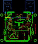
A few months ago I made pcb for this amp out of curiosity (according to the original scheme).
Trafo 2x20V 300VAC, 2SC5200+2SA1943+MJE15035/34 from Mouser. Other elements are standard 1% Beyschlag resistors and caps from Panasonic/Rubycon/Nichicon.
DC offset after +-20min warming was 13 and 15 mV. Thanks to helitrim (2k) I added in parallel to R6 (1k2) i set it up to 0V.
Q5 and Q9 coupled with a piece of copper sheet.
Attachments
I didn't have any issues with the initial turn on or biasing.
I followed the test procedure laid out in the p3a article.
Bias was set at 75ma.
The amp played music normally when connected to my test speakers. It even made my test speakers sound surprisingly good.
At this point were you getting the same volume on the speakers from both channels? Previously you stated that the left channel was resistricted to 3 V RMS.
In post 240 I included an image attachment forthe Silicon Chip Class A which has some differences to P3A such as current mirrors and CCS loads forVas collector load. I would have though the heart of the circuit could be used with changes to accomdate a bootstrap collector load for the VAS remove the current mirror in the LTP and draw connecting lines in place. I can post a component side view with tracks shown underneath and the copper side if that would help.A little bit of tidying and the addition of the jumper to resolve the 2nd stage of decoupling before the ground star.
View attachment 1221731 View attachment 1221730
I'll quote the BlackSheep: If the P3A doesn't sound good, you've done something wrong son.Thank you for setting the record straight.
Ok guys, according to the track and trace, I should have BD139/140 by Friday.
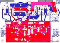
While waiting, I've been fiddling with the layout some more. Since the previous layout seemed to not be preferable, I've gone back to basics.
I've chopped off the the extra decoupling stages and gone back to a plain old Rod Elliot style layout.


This is pretty darn similar to Rod's layout however he biggest difference is the extra degen resistors, the larger input cap, larger diameter decoupling caps.
I understand that Q9 should be mounted as close as possible to the Tj of Q6 which I would take to mean the metal tab side of Q6.
However I of course want the metal tab side of Q6 on a heatsink.
Am I over thinking this, should I just be cable trying Q9 to the 'front' side of Q6 and forget about it?
While waiting, I've been fiddling with the layout some more. Since the previous layout seemed to not be preferable, I've gone back to basics.
I've chopped off the the extra decoupling stages and gone back to a plain old Rod Elliot style layout.
This is pretty darn similar to Rod's layout however he biggest difference is the extra degen resistors, the larger input cap, larger diameter decoupling caps.
I understand that Q9 should be mounted as close as possible to the Tj of Q6 which I would take to mean the metal tab side of Q6.
However I of course want the metal tab side of Q6 on a heatsink.
Am I over thinking this, should I just be cable trying Q9 to the 'front' side of Q6 and forget about it?
- Home
- Amplifiers
- Solid State
- Stability testing my new Rod Elliot P3A