Ideally, the driver is mounted to a small heatsink and the bias transistor mounts onto the back of the driver. This is where using a BD139 for the bias transistor would make mounting a little bit easier.
In one part this discusses a situation where the amplifier heats up at high output levels and then abruptly drops to a lower level. If the diodes cool while the heat in the Power Transistors lingers, because dissipation is not instantaneous as music can be, then the diode bias will increase due to less heat in the vbe. Ideally the cooling rate in the vbe should be instep with the heat sink maybe as in the Class A circuit which is a Class B on steroids.
These problems can be solved by the right size heat sink and emitter resistor values. That some builders have success while others miss the bus could experience this problem.
Not sure that thermal tracking can ever be 100%. I do not recall that particular application note, though I may have read it at one time. This is the advantage of using CFP output stages that the power transistor junction temperature is less critical. If they were hot and then the signal reduces, the local feedback around the emitter resistors largely compensates for any current change. Your point about keeping the bias device(s) in thermal contact with the output stage is why it is simpler to use the CFP configuration and thermally connect the drivers to the bias stabiliser transistor. The drivers need to be on a small heatsink even if a simple aluminium plate anyway, as this will help to keep their junctions cool. If they share the heatsink with the bias stabiliser, they all need to be mounted with the metal thermal pad pointing to the heatsink but insulated with a mica or silicone insulator, of course.
If a conventional EF2 configuration is used, then my recommendation is to mount the drivers, power transistors and bias regulator all on the same (power) heatsink. If the power transistors suddenly cool off, the heatsink temperature will still be high and the bias regulator, and drivers will still provide a reasonable stability of bias current.
The point I think you are alluding to is that ONSemi's Thermal Trak devices ought to be used more often, but I've not found any issues with the EF2 arrangement I have mentioned.
I have built this circuit with heat tracking and without not much diff in sound or scope traces. Rod clearly mentions not to share a heat sink with one of the VAS transistors. I see people doing it anyway.
It foxes me how anybody could have an issue with Rods design. It works on some of the crappiest build PCBs.
Check out my post Comparing schematics. And the TGM8 thread its similar to what your trying.
They have taken a P3A concept added stuff like speaker protection and made a gazillion improvements.
The kicad files have been shared along with the spice file.
Though I have not been able to get the spice file to run.
Ive been stuck in the P3A world for sometime now.
Have a collection of PCBs going. And even modding some of them.
Here you go.
https://www.diyaudio.com/community/threads/comparing-p3a-schematics.403881/
Need I worry about the voltage rating of the cap across C to E of the bias transistor Q9?
I salvaged some 104J film caps of an unknown voltage rating from a faulty CD player.
They JUST fit underneath the board without fowling anything.

I salvaged some 104J film caps of an unknown voltage rating from a faulty CD player.
They JUST fit underneath the board without fowling anything.
Last edited:
Need I worry about the voltage rating of the cap across C to E of the bias transistor Q9?
no, that bit of the cct has only a few volts across it.
no, that bit of the cct has only a few volts across it.
G'day Guys,
BD139/140 arrived and installed.
0.1uF film caps were soldered across Q9.
The first round of tests as per Rod's article have been passed:
1) startup with safety resistors
2) Left channel 2.5mV dc offset, Right channel 12.0 mV
3) test with test speakers: Music comes out of the speakers.
There isn't enough time left this evening for biasing. Time allowing, tomorrow I will bias up and start testing on the scope.
It was suggested somewhere early in this thread that a 4ohm load is not ideal for initial stability testing on a scope.
Would a 1k 10w cement type wire wound resistor be a more appropriate choice?
You should set the bias current with the 100R safety resistors in place. You can deduce the current level by measuring the voltage drop across either of these from Ohms law. In this case divide the measured voltage by 100. This should be adjustable up and down initialy set the trimpot for maximum resistance before power up. Then moisten your finger and while keeping your hand on the power switch bring your finger close enough to the body of either safety resistor to sense any significant heat rise.
If none adjust the trimpot so the voltage drop across either safety resistor is around 5 volts indicating a standing current of 50 m.a. If all is well adjust the trimpot for minimum voltage drop across the safety resistors and switch off, replace the safety resistors with fuses and adjust by measuring the voltage drop across the 0.33 R output resistors. dependent on what output standing current level you decide to use.
It will be necessary to check these measurements preiodically as the amp warms up.
I set the bias over a period of 45 mins.
I set the bias to 25.0mV. Bias was stable within +/- 0.1mV over 10 mins after being set.
The coupled pair of Q6/Q9 is running at about 40c according to an IR thermometer about 5cm from the transistors
The outputs are sitting at 32c.
Dc offset was 3.3mV left channel, 16.7mV right channel after biasing.
Tonight I will get the scope out again.
Are your measurements without a dummy load on the output. If Q6/Q9 are running at 40 degrees C and Q7 while Q7/Q8 are at 32 degrees C that is odd. The junction temperature of Q6 is likely to be far higher than 40 degrees C by IR thermometer.
I suggest measuring voltages across R12/R11 and deduce current levels from Ohms law i.e. divide each these voltages by the value of 220R. (V/R). Allow time for warm up monitoring for 5 or so minutes. Check also R12/R11 are really of the correct component value. If you do any scope tests then put your 1k resistor in series with your probe. The output of the amplifier is still an input to the Inverting side ofvthe LTP.
As a matterof interest for an effective Vbe the divider elements R16 and VR1 need to conduct a tenth or less of the collector and emitter currents. The Vbe transistor also needs a minimum current gain of 100.
Last edited:
It foxes me how anybody could have an issue with Rods design. It works on some of the crappiest build PCBs.
Check out my post Comparing schematics. And the TGM8 thread its similar to what your trying.
Yes, here is an example:
Long leads connecting everything together with parasitic capacitances everywhere (and inductances). Seems to work very well. Very sad😢 that others are having problems constructing this amp.
Can you please post the link to the kicad files. I can find gerbers, but not the original kicad file.
Last edited:
I guess the bigger problem might be inductance of leads...parasitic capacitances
Re your post 290. I had correspondence with Gareth Ingram at the time he was working on his TGM8 project and drew up a Tian Plot on this. His Vbe circuit divider resistors have identical value at 1k5 an arrangement that results in 2 diode voltage drops . I noted at the time that Gareths amplifier was stable in simlulations and he was happy with his results. There was no C6 Miller cap in his circuit which I will check and confirm tomorrow.Yes, here is an example:
View attachment 1224836
Long leads connecting everything together with parasitic capacitances everywhere (and inductances). Seems to work very well. Very sad😢 that others are having problems constructing this amp.
Can you please post the link to the kicad files. I can find gerbers, but not the original kicad file.
Motorola Application Note AN484A gives examples of CFP circuits, none of which uses a Vbe multiplier - just a single pair of diodes.
Setting the bias for the output stage then rests on a simple process of selecting the right values for R9/R10 for the current flow through these to paired temp sensing diodes.
R11/R12 are 220R. I checked the exact value on R11 on the left channel it was 223.4R. Me being me, I would have matched the right channel.Are your measurements without a dummy load on the output. If Q6/Q9 are running at 40 degrees C and Q7 while Q7/Q8 are at 32 degrees C that is odd. The junction temperature of Q6 is likely to be far higher than 40 degrees C by IR thermometer.
I suggest measuring voltages across R12/R11 and deduce current levels from Ohms law i.e. divide each these voltages by the value of 220R. (V/R). Allow time for warm up monitoring for 5 or so minutes. Check also R12/R11 are really of the correct component value. If you do any scope tests then put your 1k resistor in series with your probe. The output of the amplifier is still an input to the Inverting side ofvthe LTP.
As a matterof interest for an effective Vbe the divider elements R16 and VR1 need to conduct a tenth or less of the collector and emitter currents. The Vbe transistor also needs a minimum current gain of 100.
I didn't bother to measure R12 on either side. They are RN series that say 220 so that was enough for me.
I am getting .590V across R11 giving 2.7mA and .582V across R12 giving 2.6mA.
Well, first round of scoping went without any smoke.
It looks like I still have a power oscillator though....
Load is 3x 3.3K 5W wirewound resistors in parallel for 1.1K
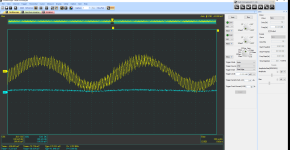
Left channel 1KHz sine wave.
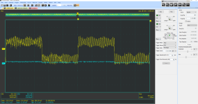
Left Channel 1KHz square wave.
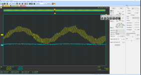
Right channel 1KHz sine wave.
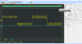
Right channel 1KHz square wave.
Compared to the first version I have:
changed the drivers/voltage gain transistors to BD139/140
Changed C4/C6 to a 220pF c0g ceramic
Put a 0.1uF film cap across C-E of Q9
It looks like I still have a power oscillator though....
Load is 3x 3.3K 5W wirewound resistors in parallel for 1.1K

Left channel 1KHz sine wave.

Left Channel 1KHz square wave.

Right channel 1KHz sine wave.

Right channel 1KHz square wave.
Compared to the first version I have:
changed the drivers/voltage gain transistors to BD139/140
Changed C4/C6 to a 220pF c0g ceramic
Put a 0.1uF film cap across C-E of Q9
Where are you connecting the probe gnd clip to? It should be on the ground side of the load when looking at the output.Well, first round of scoping went without any smoke.
It looks like I still have a power oscillator though....
If you short the probe point to the probe clip (probe GND) does the CRO display a clean flat 0 volt signal?
Connect the channel 2 probe to the input and display that as well. Make sure your input test sine wave is clean.
If you short the input to ground what does the amp output look like? Is it about zero VDC with nothing else?
Then connect the probes to the rails and look at those. Make sure the voltage rails are clean.
Try a couple of different CRO probes when doing measurement (Just in case the probe is bad). Try doing some measure without the probe. Just run some wire from the CRO directly to the AMP.
Last edited:
You said in a recent post
3) test with test speakers: Music comes out of the speakers. Does the quality of this compare with the other "working channel". If not you can cross reference circuit voltages, and temperatures of transistors to find any areas of difference to investigate.
3) test with test speakers: Music comes out of the speakers. Does the quality of this compare with the other "working channel". If not you can cross reference circuit voltages, and temperatures of transistors to find any areas of difference to investigate.
Re my post 297 (timed out)
It would be useful to print out a copy of the circuit diagram and write these for the working channel down on the printed image.
When measuring voltages connect one probe to a point that is earthed and use the other to measure voltage this is safer and quicker.
With resistors measure both ends and do a separate take to calculate resistance and vbe values.
It would not be hard to create a spreadsheet to record and calculate the details.
When I do repairs I download a parts list and a circuit diagram to work with and write measurements on the schematic and keep this for reference purposes.
This work method avoids using the probe and calculator in single steps. which involves swapping hand movements and the risk of accidental damage to components.f no
When done with this measure the subject channel. If you are lucky you might not have to look too far if there is a fault.
If none the peace of mind will have been worth the effort.
The measurements were taken from the speaker jacks.Where are you connecting the probe gnd clip to? It should be on the ground side of the load when looking at the output.
If you short the probe point to the probe clip (probe GND) does the CRO display a clean flat 0 volt signal?
Connect the channel 2 probe to the input and display that as well. Make sure your input test sine wave is clean.
If you short the input to ground what does the amp output look like? Is it about zero VDC with nothing else?
Then connect the probes to the rails and look at those. Make sure the voltage rails are clean.
Try a couple of different CRO probes when doing measurement (Just in case the probe is bad). Try doing some measure without the probe. Just run some wire from the CRO directly to the AMP.
The ground clip was attached to the chassis rather than ground side of the load.
The blue line in the screenshots above I'd the 2nd channel of the scope on the input. I can't get any higher resolution than that at that signal level sadly.
Tonight is board game night with my wife so I will run some more tests tomorrow.
I (perhaps unwisely) changed both channels to the new transistors/caps.You said in a recent post
3) test with test speakers: Music comes out of the speakers. Does the quality of this compare with the other "working channel". If not you can cross reference circuit voltages, and temperatures of transistors to find any areas of difference to investigate.
Both channels appear to be behaving the same so far. Both possibly oscillating, more testing will tell.
Your printout of the schematic idea is good. I will do this with further testing.
- Home
- Amplifiers
- Solid State
- Stability testing my new Rod Elliot P3A