Regarding #6 above, the drivers need to be on a separate heatsink from the output devices, and bias transistor transistor Q9 needs to track the drivers, not the output devices. With a EF output stage, the bias transistor must track the output devices. But in a CFP output stage, the bias transistor needs to track the drivers which should be isolated from the output device heatsink.

The energy use of the driver transistors varies very little from low to high power while the power transistors output energy consumption varies greatly under the same conditions. This is illustrated in two attachments so you can see for yourself. This is only the top half of the circuit the bottom half will be similar.
The Silicon Chip CFP Class A amplifier which could operate in Class AB places the Vbe transistor against the heat sink.
The Motorola application notes CFP designs use a special dual diode that has low VF an MSD7000 which is available in surface mount packages. If one looks at the specs it will be seen that this is not a run of the mill device. These devices are deployed on the pcb for these projects and can be used for short circuit protection purposes as well.
Attachments
That contradicts everything I had read on CFP output stages. Here is a quote from Douglas Self's Audio Power Amplifer Design book:
He goes on to explain that the Vbe-multiplier transistor needs to sense the drivers junction temperature.
In the CFP Configuration, the output devices are inside the local feedback loop, and play no significant part in setting Vq, which is dominated by the thermal changes in the driver Vbes.
He goes on to explain that the Vbe-multiplier transistor needs to sense the drivers junction temperature.
Q9 does not act as a Vbe multiplier in my simulation. The representation is of two series diodes which Rod Elliott tried and dismissed in a previous incarnation of P3A. This is less effective in controlling current than a proper Vbe multiplier.
I had looked at this earlier however that would have entailed reducing the bootstrap resistors in value from 3k3 to 2k2 to allow a Vbe multiplier to fit in without the influence of Q6 and C6 on the positive feedback connection from the bootstrap collector load. This arrangement being a blanket cover for various output transistors. I changed the Vbe transistor to a BD139 so this could sense the heat whether from the driver or the main heat sink. The comment about Vbe's is mentioned in the Silicon Chip article " bias stability in current feedback pairs is quite good even without tight thermal coupling" and "In practice VR1 (trim pot) is adjusted not to produce a particular voltage across the multiplier but to set the quiescent current in the output stage." In this instance the Vbe transistor is a few millimeters away from the main heat sink and not in physical contact.
A revised version with Vbe included is attached. The values in the base emitter connection need to have adjustment range set according to desired Iq.
Attachments
Last edited:
That contradicts everything I had read on CFP output stages. Here is a quote from Douglas Self's Audio Power Amplifer Design book:
He goes on to explain that the Vbe-multiplier transistor needs to sense the drivers junction temperature.
That make sense but if the drivers have their own heatsink then nothing will be tracked since their temp wouldnt rise accordingly to the output power, if they are in the same heatsink as the power devices then tracking will be more efficient, FI if the power devices heats up a lot they will heat the drivers and the tracking device accordingly.
More generaly i m not a fan of this kind of output stage, beside Self once provided measurements that hjow that dual EFs have quite lower distorsion at low power levels.
For an CFP output stage, the drivers and output devices must be separate. The drivers should not be the same heatsink as the output devices.
In addition the Douglas Self commentary on this, Rod Elliott states:
You can test this in LT Spice. Do a DC sweep with the bias transistor tracking the output device temp. You will see that it overcompensates the bias as temp rises.
In addition the Douglas Self commentary on this, Rod Elliott states:
Note that there is a major reason that P3A is different from most amp projects you will see on the Net - it uses complementary feedback pairs (aka Sziklai pairs) for the output stage, and quiescent current is controlled by the driver transistors. If the bias servo is mounted on the heatsink, it will provide over-compensation and crossover distortion will result.
You can test this in LT Spice. Do a DC sweep with the bias transistor tracking the output device temp. You will see that it overcompensates the bias as temp rises.
Silicon Chip had the Vbe transistor mounted on the heatsink in previous project circuits but they recanted for the one I referenced. which runs in Class A where this was close to the main heat sink with a small air gap where the will be an updaft passage of cooler air. This arrangement did not result in over correction of the Vbe in this amplifier as would be the case with intimate heat sink fastening. I would avoid this, and strapping to a driver which has a switching function. Close but not touching might be enough.
G'day Guys,
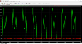
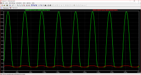
My new sig gen arrived so I fired it up. It does seem a little cleaner on the square wave,

The sine wave is about the same

So here is the output of the amp with the new sig gen.


1kHz square and sine. Things look much the same as before.
So I tried removing the cap across q9:


Not much change, perhaps the square wave is slightly better with the cap across Q9 removed.
Tomorrow night I will increase the size of C2 and see what happens.
My new sig gen arrived so I fired it up. It does seem a little cleaner on the square wave,
The sine wave is about the same
So here is the output of the amp with the new sig gen.
1kHz square and sine. Things look much the same as before.
So I tried removing the cap across q9:
Not much change, perhaps the square wave is slightly better with the cap across Q9 removed.
Tomorrow night I will increase the size of C2 and see what happens.
How does that stack up against the wave forms of your commercial amplifier.
The overlay of grass on the latest tests is no significant improvement. I have simulated the circuit as per post 1 and others have commented their builds have met with success.
If you have constructed the modules correctly which seems to be the case then there is an issue elsewhere such as the board you designed to house the power supply capacitors, and the general layout. I suspect the latter of the two and raised a couple of points in post 311 - these appear to have not been taken into consideration.
Last edited:
If you would post a photo of your chassis as it looks now so observers (plural) would be better able to comment.
It appears that your intended use is in the home and not at a public venue, In that case a single pair of output transistors would be adequate for 8 Ohm loads.
Some of your tests involve 4 Ohm loads with parallel capacitance which suggest an electrostatic speaker or a car subwoofer. If so you would have to consider doubling up on the output devices.
There is no volume control or input selector function. The first of these has an impact on the low pass filter roll off frequency. Is there a separate circuit to handle these functions and if so what does it look like.
Last edited:
The intended use here is as a stand alone power amplifier driven by a preamp of some kind.
Intended usage is home usage.
My intention with this testing is simply to make sure the amp is stable difficult loads.
My speakers are 4 ohm book shelves.
I am currently using an 6SN7 aikido preamp and an active crossover to route LF to a subwoofer.
I also use a simple OPamp preamp using LME47920.
The crossover has an output impedance of 50ohm.
The general usage of this amp would be a fairly light load as I don't listen loud and the 4ohm bookshelves aren't doing much below something like 75hz.
But i would like to have confidence that it won't blow up.
By moving to the BD139/140 I seem to have gotten rid of the oscillation, the next challenge is to get rid of the 'grass'.
I'm confident enough at this stage that with some finesse it should clean up.
Give me a week or 2 and I will have a draft layout in the new chassis.
I've got some cutting and drilling to do before I can get very far.
Hi Sadface
I am not an expert...i am starting to try and learn about amps - now AB amps.
what i read is that some BD140/139 are not stable (fakes) and it is maybe good to try the less hfe version 139/140 -25 or use the To126 TTA004B or KSA1381ESTU.
Did you try to make the C3 as big as possible? just an idea.
kr
Chris
Here's a draft layout.


I think I need to flip the to amp boards around so that the power supply connections are closer to the PSU output. That way the input wiring doesnt have to cross the psu wiring.
I am waiting on a ground lift pcb to arrive. It makes sense to me to place it right beside the PSU output.
As indicated in yellow.
I will fold up a steel shield to go between the mains side and the signal side as indicated in yellow.
A ferrite sleeve at emitter legs of BD transistors should solve oscillation problem.
https://eu.mouser.com/ProductDetail/80-B-20L-48B-L
Another way is to insert 10 Ohm resistors at BD emitter connections.
https://www.diyaudio.com/community/...compensate-for-stability.389509/#post-7104941
https://eu.mouser.com/ProductDetail/80-B-20L-48B-L
Another way is to insert 10 Ohm resistors at BD emitter connections.
https://www.diyaudio.com/community/...compensate-for-stability.389509/#post-7104941
I have used ferrite beads in preamp input and leads in my home diy projects. These units were stable without these in circuit but with the beads the sound is more like having a live artist performing in the room. Local NZ supplier Jaycar catalogue reference is LF1250.
I recommend increasing C2 from 100pf to 1nf with MKTdielectric Jaycar cat no. RM 7010. For internal wiring I use Mogami "Neglex"2534 an oldie but still of a good standard. I bought this from "Mighty Ape" a music entertainment supplies outlet in NewZealand..
I recommend increasing C2 from 100pf to 1nf with MKTdielectric Jaycar cat no. RM 7010. For internal wiring I use Mogami "Neglex"2534 an oldie but still of a good standard. I bought this from "Mighty Ape" a music entertainment supplies outlet in NewZealand..
So your ears can hear 159kHz? Remember, that's the -3db frequency, not an absolute cutoff point. This amplifier is like a barn, with the doors wide open. It'll pick up all kinds of interference. 1nF is a more appropriate value. Most source impedances are in the 50 to 100 ohms range.
- Home
- Amplifiers
- Solid State
- Stability testing my new Rod Elliot P3A