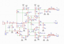
I think that would be a great idea for someone learning to build and design amplifiers. Add some parts, get it working and stable, and find out if they can hear (and like) the difference.
Rod designed the P3a for his purposes. He places great importance on minimizing parts count. This won't be important to everyone. I also understand he originally used this design as a PA amp and built them in great numbers.. hence a low part count kept the costs. He also mentions that the P3a doesn't like inductors and states that he doesn't fully understand why.
The last comment is strange as loudspeaker crosover networks use inductors and the speaker coils are also inductive. There was a small coil in series with his P3 circuit which has not been carried forward into his P3A. Crossover networks vary in design, and while the P3A may able to handle most it would seem there are others that upset this amplifier.
Last edited:
He’s saying that CFP output stages can run at lower bias levels that EF output stages. But the range of the bias for lowest distortion is much narrower with CFP. If you have a 1k pot and the range you’re tuning to is 50R, it’s hard to set and tune this with a 1 turn pot.
G'day Guys,
Here is my first draft of a pcb layout to accommodate the stability improvements etc.
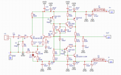
Schematic: I'm not sure if C-5/C-6 are of much importance so I haven't yet put them in the pcb.
From what I can work out the positive rail is more important here.
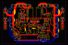
This is just a first draft, things like labeling, trace width, pad sizes, extra pad options etc are not yet optimised.
At this stage I am concerned with trace routing and parts placement.
This is loosely copied from Rod's part placement for Q4-Q9, VR1 and R13/R14. The rest is just where it made sense to me to put it.
Here is my first draft of a pcb layout to accommodate the stability improvements etc.

Schematic: I'm not sure if C-5/C-6 are of much importance so I haven't yet put them in the pcb.
From what I can work out the positive rail is more important here.

This is just a first draft, things like labeling, trace width, pad sizes, extra pad options etc are not yet optimised.
At this stage I am concerned with trace routing and parts placement.
This is loosely copied from Rod's part placement for Q4-Q9, VR1 and R13/R14. The rest is just where it made sense to me to put it.
Sorry I only got to page 5.
But just wanted to say I had a very similar exp with my first attempt of the P3A (Not rods PCB).
And all my problems were caused by defective / fake components.
This design is bullet proof. It will work out the box even on a bread board.
I blame myself for not following rods advise which was
1. Use a power limiting resistor for first time power up. you will never blow anything making testing and trouble shooting fast. Yes somebody has already pointed this out. But its critical advise.
2. I noticed a few different values being tossed about its not 75 its 50Mv for class a/b and 150 ohms for class A.
3. The gain goes up with tmep. The temp is based on how hard you push the amp your basic heat sink size. This drove me mad. My solution is to turn on the fan at say 60c turn off at 40C this keeps my bias values in chk no matter how hard or soft I push the amp. I use a i3 intel fan 2$ and a Temp control circuit for 2$.
Not sure building a new PCB makes any sense. If the basic design on Rods PCB is not working.
I would not change the design till each change was verified. In the sim and a bread board.
Maybe I should have read pages 5-9 will do when I get back from work.
Last edited:
Why me? Why are you asking me all these questions?For what reason? The last repair I did with blown driver and output transistors was in a standard Darlington. The trimmer for the Vbe bias set was a single turn trimmer. This was a Sansui amplifier classic? The same applies with the Leach lowTIM amplifier I built so you are going against the late professor.
Sincerely, I have very little interest in discussing the ins and outs of EF bias and thermal compensation in Leach's amp which is completely out of topic here with the CFP P3A. Similarly, I don't really care about carbon trimmers. I haven't used them in 20 years. And finally I have a hard time making sense of your writing.
Here is the next version.
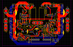
I moved a few things around to get the feedback path as short as possible.
I squeezed a few things up to generally shorten paths and fill empty space.
I added the extra decoupling caps on the negative rail since there was plenty of space on that side of the board.
Schematic for reference:
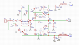

I moved a few things around to get the feedback path as short as possible.
I squeezed a few things up to generally shorten paths and fill empty space.
I added the extra decoupling caps on the negative rail since there was plenty of space on that side of the board.
Schematic for reference:

Try genuine BD139-140If you are asking me:
Fairchild: KSA1220/KSC1690
Fairchild 2SA1943/2SC5200 for the outputs.
Last edited:
Sadface, it is quite probable the amp will not work as it should using the KSA1220/KSC1690 transistors, resulting in a 'sadface' when u try it out.
I tried the P3a in the LTspice simulator with these transistors, and indeed it started behaving crazy when cranking it up.
As thimios says, use bd139/140. Cheap and reliable. And they are still being made, and probably will be forever. Or MJE15034/15035
I tried the P3a in the LTspice simulator with these transistors, and indeed it started behaving crazy when cranking it up.
As thimios says, use bd139/140. Cheap and reliable. And they are still being made, and probably will be forever. Or MJE15034/15035
Last edited:
Exactly, Rod also advocates BD139/40 for P3A drivers. For VAS we may try Low Cob transistors instead of BD140.
You could try KSA992 for the driver. It is pinout compatible with BD140.
Mooly uses TO-92 devices in his ±45V amp, which run right at their thermal limit and is a proven design. Might be interesting to give KSA992 a try.
Mooly uses TO-92 devices in his ±45V amp, which run right at their thermal limit and is a proven design. Might be interesting to give KSA992 a try.
For P3A VAS i hve Sanyo 2SA1209 so why use to92 ?! But it's true that today we don't hve much choice in through hole to-126.
I mention KSA992 as a device readily available that fits the existing pinout. KSA1381 would also be an option in a TO-126 package. Though the Cob on KSA992 is lower.
I ran a sim and it dissipates 178mW. If you bump the rails to 40V for worst case mains and xfmr regulation, it dissipates 234mW. It has a 250 °C/W thermal resistance to ambient. At 234mW, its derated power limit is 260mW (if my math is correct). So still a bit of safety margin.
In sims, the 1K/1W THD amount doesn't change much, but it shifts from odd order dominance to even order dominance.
Sims also suggest that you can add a 100n cap across on the bias transistor Q9 and remove C6 (as previously discussed)
In many other threads, builders have dropped C4 from 100p to 68p with success. Simulation loop gain and square wave analysis backs this up.
In many other threads, builders have dropped C4 from 100p to 68p with success. Simulation loop gain and square wave analysis backs this up.
I've also previously mentioned the benefits of a current compensation resistor for the bias generator. Here are some graphs to illustrate its impact on bias stability as supply voltage changes. However, this one is tricky to implement without PCB changes.
Attachments
- Home
- Amplifiers
- Solid State
- Stability testing my new Rod Elliot P3A
