Hi Sheldon
What was the reason to omitt cascodes in a first place? Now in this case you can omitt zeners too, but than you have to supply CSS-s from +/- rails.
In your current schematic proposal you get lower PSRR, higher power dissipation practically on every active part of the front-end, higher temperatures, more drastical temperature variations from a cold start and in a signal terms you gain nothing. If it would be like going into simplest version of them all, than it would be understandable, but here with triple output sophisticated version I would kindly suggest you to follow more Bigun's sch.
Regards, Andrej
Attachments
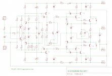
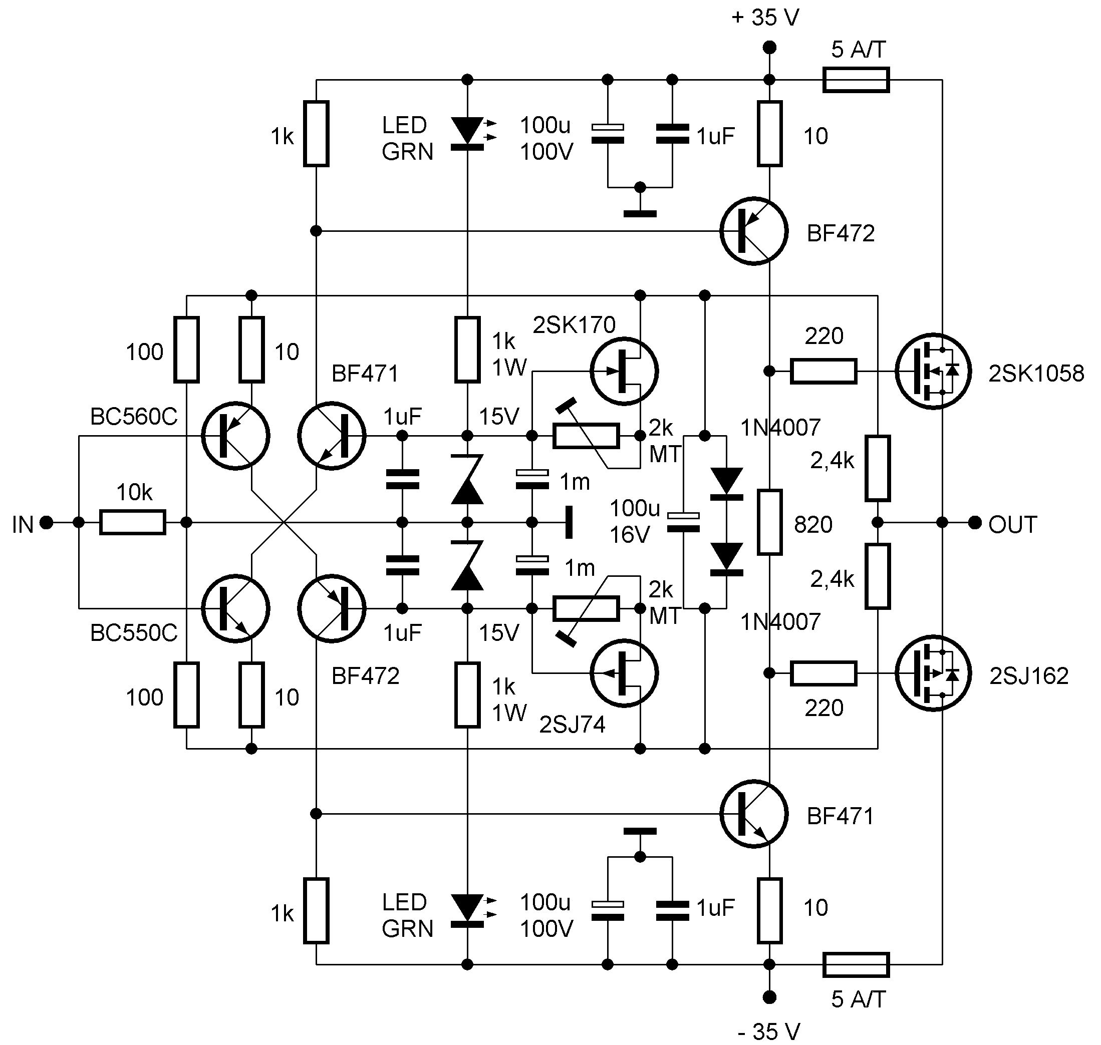
Glad I asked. Show what happens when a rank amateur plays. Good thing it's only lines on the screen. OK, front end from post 1339 in the SSA thread (except non complementary current source pair) http://www.diyaudio.com/forums/atta...ymetrical-amplifier-ssa-amp-basic-mos-fet.jpg - back end from Mihai:
Note: Looking at the top half, I tried to copy your current source LC, but it seems reversed to me. Have I got that wrong?
Sheldon
Note: Looking at the top half, I tried to copy your current source LC, but it seems reversed to me. Have I got that wrong?
Sheldon
Attachments
Last edited:
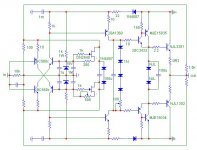
Sheldon, is your top branch depletion CCS correctly oriented?
I don't think so, but I copied LC's orientation. I think they might be reversed on that schematic. I think it should be like this:
Sheldon
Attachments
Last edited:
I don't think so, but I copied LC's orientation. I think they might be reversed on that schematic. I think it should be like this:
Sheldon
No, I use p and n channel J-FET's but as I see I somehow reversed the p and n position.
Look Sheldon If you would still like to omitt cascodes from input pair, there is already tested solution from Christophe's (Esperado) Crescendo sch. Only that instead MOS-FET output stage you can incorporate output triple BJT stage.
P.S. Christophe did a great job on implementing SSA bridge feedback to a standard, most common front-end. In this way any symmetrical front-end can be SSA modified to low Z (current) feedback. Advantages are quite obvious from his measurements and subjective listening experiences.
Attachments
Last edited:
No, I use p and n channel J-FET's but as I see I somehow reversed the p and n position.
Sorry if I was not too clear. I copied the top half of your schematic, but used depletion mode devices for both top and bottom.
Look Sheldon If you would still like to omitt cascodes from input pair, there is already tested solution from Christophe's (Esperado) Crescendo sch. Only that instead MOS-FET output stage you can incorporate output triple BJT stage.
I am not against the cascode, just playing with the schematic to understand the possibilities. Is the last version I posted OK, at least in principle?
Sheldon
Sorry if I was not too clear. I copied the top half of your schematic, but used depletion mode devices for both top and bottom.
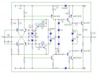
Yes, both n type fets as adjustable current sources. They're well placed in your sch, only that I don't know if 1k gate resistors are necessary in CSS.
I am not against the cascode, just playing with the schematic to understand the possibilities. Is the last version I posted OK, at least in principle?
Sheldon
Sch is in general OK, only in series with two NJL diodes there should be a resistor defining correlation between driver-output quiescent currents. Now as it is, the amp would be B-class biased no matter of the 100 ohm trimmer resistance setting.
Yes, both n type fets as adjustable current sources. They're well placed in your sch, only that I don't know if 1k gate resistors are necessary in CSS.
Others have recommended stoppers for the DN2540, due to the high transconductance. I'm not qualified to judge, so put them there as a precaution.
Sch is in general OK, only in series with two NJL diodes there should be a resistor defining correlation between driver-output quiescent currents. Now as it is, the amp would be B-class biased no matter of the 100 ohm trimmer resistance setting.
That's true at low currents through the TT diodes, but apparently not at higher currents. See my post 138: http://www.diyaudio.com/forums/soli...imple-symmetric-amplifier-14.html#post2775971
It seems the TT diodes were selected for use with lower currents in mind.
Mihai originally specified 75 or 100mA through the CFP. At those currents through the TT diodes, the outputs are biased well past the "optimal class B" bias with 0R2 emitter resistors. So the output bias can be regulated by adjusting the current through the CFP, or emitter resistors, or?
As always, I'm open to be corrected on this.
Sheldon
Last edited:
I had the 2540s in cascode CCS mode with 100R gate stoppers and HV across working clean, but others had reported bad problems when used as CCS anode load and had to go >1K. Just mentioning so you may test lighten the value later since it compromises the CCS HF PSRR in synergy with the 200-300pF Ciss (tends towards max with only 12-15VDS anyway).
I had the 2540s in cascode CCS mode with 100R gate stoppers and HV across working clean, but others had reported bad problems when used as CCS anode load and had to go >1K. Just mentioning so you may test lighten the value later since it compromises the CCS HF PSRR in synergy with the 200-300pF Ciss (tends towards max with only 12-15VDS anyway).
Thanks Salas, I'll play with that when I build. I've got enough that I could actually cascode them. Seems a bit overkill for this.
Sheldon
Here shows the decrease in RR as frequency increases above about 10k. However, it's still 90dB at 200k. Do we need better than that? After all, the resistor it replaces only offers little RR.
http://waltjung.org/PDFs/Sources_101_P2.pdf Figure 12a,b
Sheldon
http://waltjung.org/PDFs/Sources_101_P2.pdf Figure 12a,b
Sheldon
There Mr. Jung uses 100R gate stopper also. If with 1K, the up slide would start much earlier. But no, at this phase all you need to see is that the CCS substitutions help the DC offset thing. I would start conservative, and later on if there is success, see about local performance details. Beyond patching the branches for controlled current, those CCS offer more OLG (5dB) and increase PSRR for the input stage. Its not a phono, but if you want to have great PSRR in treble and beyond there are ways. You could evaluate if it matters then, its fun. But one thing at a time. 
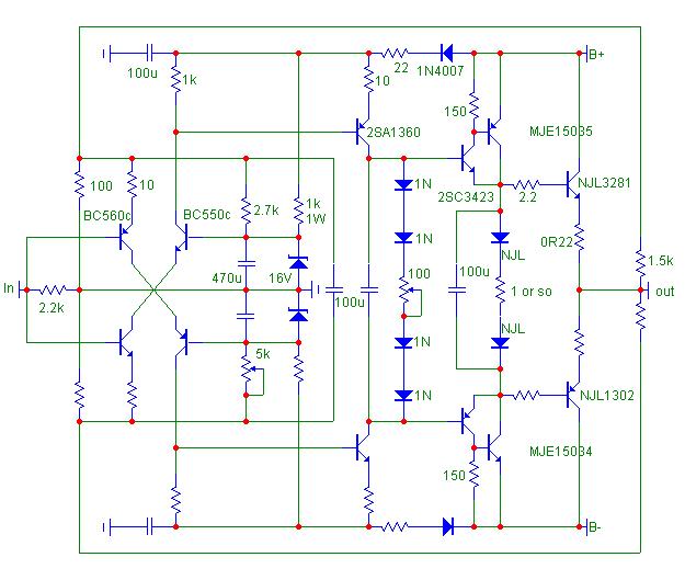
I posted what amounts to a Thermaltrak version of the TGM5 over in LC thread.
http://www.diyaudio.com/forums/atta...etrical-amplifier-ssa-mihai-output-buffer.jpg
Playing around with the TT diode bias spreader (no series resistor), I found that at about 30mA current I get about 18mV over the 0R2 emitter resistor. At 50mA through the diodes, I get about 30mV over the resistor, and at 100mA the output bias increases to about 55mV. Bias current would be 90mA, 150mA, and 265mA, respectively. Nothing earth shaking there, but here's the question:
I've read that optimal AB bias is around 18mV at the emitter. But in order to get that for this schematic, I'd have to reduce the current through the CFP driver to around 30mA. So what are the trade offs here? Or, can I just push more current through the outputs with impunity (assuming adequate cooling)? And, what should be the minimum for the CFP driver?
Digging around a little more, I think I may be able to answer my own question. I realized that this version of the FC100 output buffer differs from the original, only in that it has a single output pair. Therefore it requires only 1/3 of the drive current to the outputs. So something on the order of 30mV current through the drivers and diode bias string is plenty to maintain class A operation in the drivers. Seems like this can work out with reasonable values. Of course, I can add series resistance to the diode string if I want to use less current in the drivers, or if there is an issue with TT diode variability.
The one issue with this is that the variables (driver current and output bias) are not independently controlled, so part variability could be an issue. And I don't know if changing the driver current values will change sonics.
In summary, I think I can achieve optimal class B bias with reasonable current through the drivers, using this TT biasing technique. If I want to run much more class A in the outputs, I can either run more current through the drivers, or add some series resistance to the diode string.
Sheldon
Last edited:
Sheldon; said:In summary, I think I can achieve optimal class B bias with reasonable current through the drivers, using this TT biasing technique. If I want to run much more class A in the outputs, I can either run more current through the drivers, or add some series resistance to the diode string.
Sheldon
Hi Sheldon
That is exactly what I elaborated in my post. With resistor in series with diode string you can play to adjust optimum conditions exactly to your specific needs. You only have to decide wheather to use cascodes in the front-end or not. If you would read the last Sonya's post in a SSA thread, you'll see what can be expected regarding sound quality.
Yes, thanks. Once I realized that I can get by with much less current in the drivers than for the FC100, then biasing becomes simple. At anything over 15 or so mA in the driver, the resistor is pretty small. But a fixed resistor is fine, once testing determines the proper value.
It might take a couple of months to build, as I have to free up a chassis and power supply.
Sheldon
Hi Sheldon
Positive temperature coefficient of the Sziklai driver pair can substantially influence the output's bias current especially if their temperature dynamics is different from the output's ie. if they're mounted on a separate heatsink. If drivers are thermally separated from the main heatsink their final temperature will reach certain level (depending on power dissipation) which is far more stable than temperature variations of the main heatsink. So if they are not anymore variable in the formula, thermal track diodes themselves (or Vbe multiplier) will do the compensation job successfully. But that is only in ideal conditions when circuit is in the open air, as soon as you put PCB in a closed box, thermal variations starts to influence all active temperature dependent parts. Ideally each active and positive tempco gain part characteristics should be temperature independent, to achieve this, they have to be thermally compensated.
So yes, you can use those four diodes to thermally stabilize the drivers no matter where their installation place would be. In a case of a thermal overcompensation you can simply remove one these diodes back to the PCB.
Regards, Andrej
Last edited:
Thanks Andrej. From that description, it might be better to mount the and driver diodes on a separate sink, if that sink changes temperature less than the main heatsinks. I'll think about this some more.
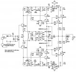
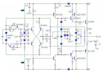
Meantime, my latest schematic versionl. May need a resistor in series with TT diodes, depending on driver current. Final determination, once assembled. Also may need compensation for the drivers. I plan to more or less follow the schematic diagram for the physical location of parts.
I've checked this, but may have some mistakes. Sometimes I have to wait a day to find them, after looking at the schematic too long.
Sheldon
Attachments
Last edited:
Member
Joined 2009
Paid Member
Sheldon,
I think the CCS devices will themselves have a temperature sensitivity; the VAS devices are also temperature sensitive, not as much as the input pair but still enough to change the current through the bias diode string. I'd run it through spice to see how all these things add up and then decide if you have the right temp comp scheme or not.
Lazy Cat,
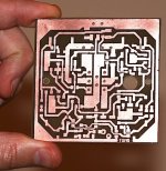
I've made some progress. I printed out my pcb design onto glossy paper, Oxford University magazine seems to work best, with printer on 'transparency' setting.
I chopped up the 6" x 6" shiny new double sized pcb into 4 equal(ish) squares and using the wife's clothes iron I transferred the pattern to the pcb (after cleaning said pcb with wire wool and acetone). It worked pretty good but I noticed two issues. a) the pattern was reversed, I forgot to print out a mirror image and b) the traces expand / squish under pressure of the toner transfer process and closed up the spaces between the legs of the SOT 363 part. I had expected I would have to calibrate the design to my production method.
So I reduced the pad and trace sizes for the SOT 363 and drove back to work to re-print it mirror imaged. The next transfer worked better and after touching a couple of spots with a marker pen and covering the backside with protective sellotape I committed it to a bath of etchant.
And half hour later the cake was baked. A clean in acetone and a shiny new board was delivered to the world I've since drilled the holes called for by the design. Photo attached...
I think the CCS devices will themselves have a temperature sensitivity; the VAS devices are also temperature sensitive, not as much as the input pair but still enough to change the current through the bias diode string. I'd run it through spice to see how all these things add up and then decide if you have the right temp comp scheme or not.
Lazy Cat,
I've made some progress. I printed out my pcb design onto glossy paper, Oxford University magazine seems to work best, with printer on 'transparency' setting.
I chopped up the 6" x 6" shiny new double sized pcb into 4 equal(ish) squares and using the wife's clothes iron I transferred the pattern to the pcb (after cleaning said pcb with wire wool and acetone). It worked pretty good but I noticed two issues. a) the pattern was reversed, I forgot to print out a mirror image
and b) the traces expand / squish under pressure of the toner transfer process and closed up the spaces between the legs of the SOT 363 part. I had expected I would have to calibrate the design to my production method.So I reduced the pad and trace sizes for the SOT 363 and drove back to work to re-print it mirror imaged. The next transfer worked better and after touching a couple of spots with a marker pen and covering the backside with protective sellotape I committed it to a bath of etchant.
And half hour later the cake was baked. A clean in acetone and a shiny new board was delivered to the world
I've since drilled the holes called for by the design. Photo attached...Attachments
Last edited:
Hi Gareth
TGM5 prototype PCB you've made is simply gorgeous, I'm impressed how good this toner transfer method is, excellent for DIY-ers. Now you are on the fast lane to make a very good amplifier. I looked over your schematic again and I don't see any problematical spots, only you will have to play a little with Miller compensating capacitors. I hardly wait to hear the news about results.
Regards, Andrej
- Status
- This old topic is closed. If you want to reopen this topic, contact a moderator using the "Report Post" button.
- Home
- Amplifiers
- Solid State
- TGM5 - all-BJT Simple Symmetric Amplifier