you miss the fact that at low supply voltage the capacitance in the gate exceeds the reference data from the datasheet.ay the output devices have 1nF of gate capacitance, and you need to charge the gate to 6V above source, that's 6nC of charge each, so 10mA can charge two of those in 1.2µs, which is fast enough for audio.
Although you yourself confirmed that the current is insufficient at a given supply voltage.
")
Nope, the order of magnitude is plenty good enough, just as it has been back from the old toshiba circuit with 2SK135/2SJ49's - when I built my first one I hadn't enough gate resistance and it oscillated heavily between 2 and 3MHz - there's enough slew rate - that amp still works fine 43 years later, although I did re-cap it a few years ago.
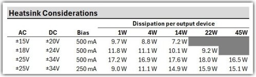
This is indeed a low power class AB design with a large class A region. With 20V rails, it should be good for 14W and run well in a 2U chassis. At 24V, it should provide around 25W. Probably still work in a 2U but possibly on the warm side.
The components in the design can work up to 35V while maintaining a decent safety margin, though bias would need to drop or a larger heatsink used.
Maybe 24V rails are a better goal. 25W of output gives 14dB of headroom at a 1W nominal listening level. Seems appropriate for efficient speakers and reasonable volumes.
I assessed the stability of the DC operating points in simulation by modeling temperature rise in the devices and varying the hot and cold states, ambient temperature and supply voltage. It all looked reasonable to me.What is the dependence of the stability of the operating point on temperature and the level of potential difference in the supply voltage buses?
My only concern is the dc offset. It showed up to 40mV of variability. This is why I included a provision for a cap in the feedback network. Most of this variability came from the cold to hot state. If it is 40mV or less in actuality, that is probably OK. But if the sim is overly optimistic, then the cap may help.
Here's some thoughts on build options...
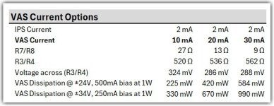
The VAS current can be adjusted by changes to R3/R4 and R7/8. You can see that with VAS currents from 10mA to 30mA and rails for 24V to 34V the VAS transistors should stay within their limits with the proposed heatsink. Might be on the hot side with the most aggressive options.
The dissipation in the output devices suggests a 2U chassis for up to 24V rails should work. With 34V it might work if the bias is reduced, but could be on the hot side if pushed hard.
Attachments
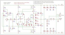
How do you like this option? (see attachment)My only concern is the dc offset. It showed up to 40mV of variability.
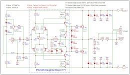
*Jfet input stage with initial current at a thermostable point
*current in the second stage is mirrored with a coefficient
*the current of the second stage is sufficient to drive the output side mosfets

Last edited:
I think the feedback cap option is simpler. I ran some more sims. Without the cap DC can fluctuate 40mV from cold to hot states. With a cap, this drops to 5mV of variation. This is assuming an actual build performs like the simulations.
Having the provision for a cap is probably a good idea. A builder can decide whether they want it based on the amount of DC offset they're comfortable with.
I also ran more sims on the feedback network to assess the size of the resistors and the feedback ratio. I think a 680R/100R combo works best. This considers DC stability, AC response, phase & gain margin, THD and noise. I also adjusted some of the other resistors to tune it a bit more.
Attachments
Just jumping back in after being away for a while. In looking at the 3D drawing of the circuit, I notice that you are considering the small "square" trimpots, which are available in either top or side adjustment. I used those for trim adjustments for span and offset in electronic weigh scale designs. I had a great deal of trouble with them; the wiper has a tiny contact area, and they would get intermittent after a year or so. They were handling voltage and currents similar to those that might be estimated in your design. I switched to the style (Bourns 3006 series) that were more rectangular and had a long screw internally to move the wiper back and forth. The design had a much more durable contact area, and I had virtually no problems with them, even after years of extended service.
Just a thought. It looks like a nice, simple design - I am anxious to see how it turns out!
Just a thought. It looks like a nice, simple design - I am anxious to see how it turns out!
in addition to brian92's comments and your own earlier comments about mosfet gate drive, why not use beefier parts for Q7 and Q22?How do you like this option? (see attachment)
*Jfet input stage with initial current at a thermostable point
*current in the second stage is mirrored with a coefficient
*the current of the second stage is sufficient to drive the output side mosfets
View attachment 1283942
why not use beefier parts for Q7 and Q22?
Hello! Q7 and Q8 operate in linear mode, with low voltage and high current, while dissipating only 16 milliwatts of power, while Q7 Q22 in hot thermal mode. stabilization is carried out due to the current mirror (see attachment).
In Briand's version, stabilization only due to the NFB and multiplying with the gain of the input stage increases the errors of this stability; his voltage amplifier operates in nonlinearity (hot mode).


You have the most complex topology, because there are few parts, and each stage operates in a nonlinear mode. It is almost impossible to select components in the model so that they simply correspond to the hardware implementation.I think the more complicated circuits on this page are far from the simple version I have posted.
thank you - this is impossibleGo back to my design.
Thank youOf course I like the fact that you are posting.
I’ll probably just read the posts in the topic when I have free time, and won’t publish anything.)))But that goes away from the topic in this thread.
Could always open your own thread because there is always room for interest in more than one topology being discussed!I’ll probably just read the posts in the topic when I have free time, and won’t publish anything.)))
Your work is always interesting to read, and so is Lineup's. Would be nice to see where both paths lead.
Here is the latest version by me:
Hi Lineup,
One cautionary note: In your design, you are adjusting the DC offset using the pot R16. If this pot fails in the open position, the amp will likely catastrophically fail. Driver current and output currents will spike. If you use the approach I am suggesting, you'll just loose your DC offset trim - which should just be 100 mV or less of DC on the outputs.
Also what it the thought behind the large output inductor? The design should be stable without it. And even if one is added, I wouldn't think it would need to be this high.
Ok.Could always open your own thread because there is always room for interest in more than one topology being discussed!
Thank you.Your work is always interesting to read
Let's look at at least one cascade using the link: https://www.diyaudio.com/community/...ut-and-lateral-mosfet-out.409798/post-7624906Would be nice to see where both paths lead.
gain of the jfet cascade U10=R13/ (R19/2) =~1, i.e. it doesn't amplify anything, is it a source follower? not like that. Maybe you know? because I don’t know why there is a cascade in the amplifier that does not amplify anything. In your opinion, this is “a different topology, a different path” - ok,
Also what it the thought behind the large output inductor? The design should be stable without it.
This is due to the capacitive load, the transient process is greatly distorted, an attempt to “protect” the NFB. The value of the inductor is too large, its tuning frequency will be less than an octave from the cutoff frequency of the audio range, and this means its influence will be audible.
- Home
- Amplifiers
- Solid State
- Ultra Amplifier with JFET input and Lateral MOSFET out