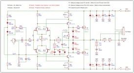
Great discussion! Brian, I like your suggestion of making two PCBs. Of course this is more work for you. But it would preserve Lineups original design and provide other options. If it would all fit on one, that would be my choice. I would want to match the Idss of N and P halves, if operated without source resistors.

Option 1: 1xLSK489 + 1xLSK689 tested
Option 2: 2xLSK170 + 2xLSJ74 tested
Option 3: 2x2SK170 + 2x2SJ74 not tested, but maybe I will
LSK170 should be like 2SK170 and LSJ74 is alike 2SJ74.
I can think of this would work:
Option 4: 2xLSK170 + 2x2SJ74
Pairs would need to be matched in options 2, 3 and 4.
Now 100% match is not needed, but close should it be.
There is possible to adjust the circuit a bit when there is not 100% match.
yep, a truly matched quad would of course be best. most diyers do some spot matching: IDSS, maybe VP, but not transconductance, any of the various capacitances, etc. true curve tracers are rare and expensive. most importantly, our resident semiconductor gurus here will tell you cannot have perfectly matched N & P devices anyway while residing in our universe (laws of physics and such), so you'll have to cheat to get good complementary matching done anyway 😈. or get a good time machine to go back to the time of the 2SK163 and 2SJ44 devices from NEC. It seems they were about the best complementary pair of low noise, high gain devices available for us regular people.

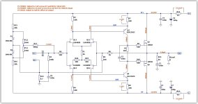
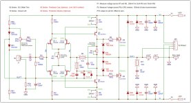
Bob Cordell discusses using LSK489/LSJ689 in his book (Chapter 9 figure 9.12). He recommends adding 100R source resistors to the LSJ689 to balance out the transconductance issues. Something like this. It seems to perform similiar to LSK170/LSJ74 in simulation.
Attachments
and if like this:He recommends adding 100R source resistors to the LSJ689 to balance out the transconductance issues.


@Hennady Kovalsky
Interesting circuit. You have added components.
Is the performance good? THD? Bandwidth?
Interesting circuit. You have added components.
Is the performance good? THD? Bandwidth?
I have added resistors like that in the sources.Bob Cordell discusses using LSK489/LSJ689 in his book (Chapter 9 figure 9.12). He recommends adding 100R source resistors to the LSJ689 to balance out the transconductance issues. Something like this. It seems to perform similiar to LSK170/LSJ74 in simulation.
I have changed the DC-offset again.
I have increased the VAS current to 10mA.
Here is the current version. THD is 0.00050%
@Hennady Kovalsky
Interesting circuit. You have added components.
Is the performance good? THD? Bandwidth?
sorry, I don't have enough time. as soon as free time appears, I will try to dial a model.
I recommend LSK489/LSJ689 TO-71 duals.Sounds like this is a case where quad matched would be preferred for best performance, but not required? This is something that is difficult to assess in simulations, as matched NPN-PNP models are not readily available (to my knowledge).
If this is the case:
- LSK489/LSJ689 is the lower cost and lower performance route (since matching the NPN to PNP is likely cost prohibitive).
- DIYAudio store quad-matched LSK170/LSJ74 is the highest cost and higher performance route.
- J113/J176 would likely be best mix of price and performance if there was a source for quad-matched devices.
They are exactly matched.
Can be bougth from NAC Semi https://www.nacsemi.com/
I think J113 works best with lower currents.Another question for the experts: We often see 2mA used for LSK170/LSJ74 IPS. Is there a similar heuristic for J113/J176?
Nelson Pass Uses 0.5mA per J113 in his DIY FrontEnd 2022.
I recommend LSK489/LSJ689 TO-71 duals.
They are exactly matched.
Can be bougth from NAC Semi https://www.nacsemi.com/
Why do you think there are exactly matched. The LSK489 and LSJ689 will be matched to each other... but that is the whole point of the duals. But even then, its not exact. The datasheet has 90% to 100% match. There's nothing on NAC's site suggesting the LSK489 is matched to the LSJ689.
Also, I would suggest buying LSK489 from DigiKey (They don't offer LSJ689). You can get it in A, B, or C grades from the them. What NAC sells is ungraded.
Finally, why are you suggesting TO-71? Most of the posts here have indicated concern over the high cost of these devices. TO-71 is 23% more expensive that SOIC yet very similar in size and pitch. Why recommend the most expense option when both are readily available?
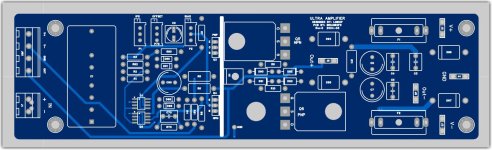
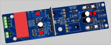
Getting closer on the PCB. Probably needs a bit of tweaking still and a check of the silkscreen elements. Also need to cleanup the pours.
A couple of notes on my thinking:
A couple of notes on my thinking:
- The values on the schematic are from my version of the design. However, the board should accommodate most of the different versions of the design that have been proposed.
- JFETS are LSK489/LSJ689 in SOIC package. The boards can be modified to use other devices in the future.
- It is designed to work with Dissipante 2U 300mm deep heatsinks. The clear space on these heatsinks after accounting for mounting brackets should be 59mm x 260mm. This board is 52mm x 192mm.
- The R7 & R8 measurement resistors have a longer pitch to allow for easier attachment of probes to the resistor leads.
- The feedback network has provision for 1W devices if the builder wants to use lower value resistors for noise considerations.
- A provision for a DC cap on the feedback network has been added (80 series numbering). It has bypass diodes to allow for a smaller devices to be used if the feedback network is low noise. It is yet to be determined if the DC offset will be stable without it. If it is not needed, the cap can be replaced with a link.
- Provisions for protection diodes and a connector for a protection board has been added (90 series numbering). These are all optional
- The bias pot bypass cap C2 has provision for polyester and electrolytic devices. This allows a higher values to be used if needed during the actual build.
- The VAS transistor heatsink uses 1/16" (1.6mm) thick flat aluminum stock. It is mounted using a Keystone 616 L bracket.
- There is a ground pad near the VAS heatsink if the builder wants to ground it.
- The extra hole near the output devices is to allow for the mounting of a temperature monitoring device. This would be used by the protection board, which is outside the scope of this thread.
- As show, it uses side adjusting pots which allows for it to be adjusted from the top when mounted in the chassis. However this would require a second PCB for the right side. I may try to do this... depends on how much motivation I can muster.
Attachments
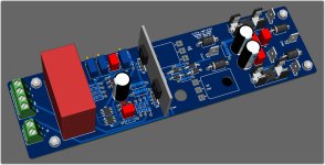
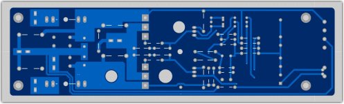
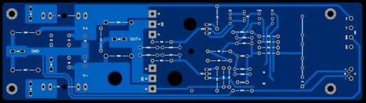
beautiful layout!Any feedback on the layout?
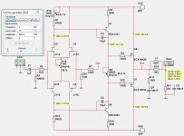
But the circuit is not ready yet, the current Q3Q4 is very weak for linear control of the output transistors, Q1 and Q2 do not amplify anything.
What is the dependence of the stability of the operating point on temperature and the level of potential difference in the supply voltage buses?
Q3/Q4 have about 10mA, plenty to drive MOSFETs, perhaps a bigger problem is the +/-20V rails giving little headroom - it takes a fair few volts to turn on laterals, with low voltages this becomes a substantial loss of output range unless the drivers have separate higher voltage rails, such as +/-25V
Say the output devices have 1nF of gate capacitance, and you need to charge the gate to 6V above source, that's 6nC of charge each, so 10mA can charge two of those in 1.2µs, which is fast enough for audio. Of course more loop gain would help stop distortion from rising at higher frequencies where the drivers work harder, but you don't have to worry about slew limiting.
Say the output devices have 1nF of gate capacitance, and you need to charge the gate to 6V above source, that's 6nC of charge each, so 10mA can charge two of those in 1.2µs, which is fast enough for audio. Of course more loop gain would help stop distortion from rising at higher frequencies where the drivers work harder, but you don't have to worry about slew limiting.
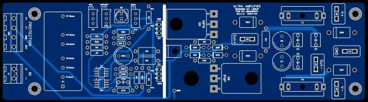
- Home
- Amplifiers
- Solid State
- Ultra Amplifier with JFET input and Lateral MOSFET out