To get dual input transistors to both contribute to the gain is an improvement.The only change I made was to the VAS emitter connections; I made no value or connection changes to offset pot that was added earlier and I performed no simulations or analysis. Just throwing it out there for discussion.
But, I have built a number of amplifiers over the years that use this topology and found that it works quite well; there's a reason it's still around ...
The same is used by Curl in his JC-2 preamp, I think.
Last edited:
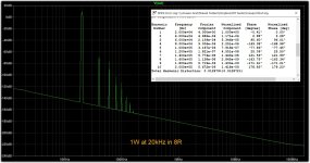
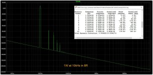
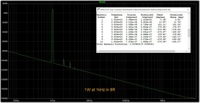
Well it isn't, look at post #18. The 7th and 9th are also a bit a bit high. I think it is the differential pairs that give the odd harmonics?but the spectrum will likely be 2nd order dominate and monotonically descending.
Don't trust simulations blindly. Look at the datasheets, yes they are a bit noisier but not 1000 times of course. Besides, you are not designing a mic preamp here.Based on a quick sim J113/J176 performs better in terms of distortion, but noise is exponentially worse... like 1000 times higher noise. I'd same this isn't worth pursing.
These don't measure well if low THD is your yardstick for performance. Yet they still appeal to many.
It seems low THD definitely is an important yardstick for the lineup designs.
If you want lower THD and a nicer spectrum, consider this one with a Hiraga front end:
Last edited:
a decrease in distortion indicates an expansion of the amplification spectrum, which is logical because “parallel amplification channel” appeared on HFNew version with Emitter VAS and DC-offset.
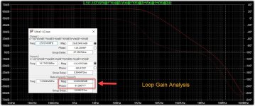
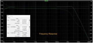
Bandwidth: 2.7 MHz
Distortion: THD 0.00049%
The dist was 0.00100% before.
but this is not an indicator of quality.
Naturally, because The band expanded and you had to reduce the gain of the input stage on the jfet at high frequencies, because the bipolar transistor in the second stage began to amplify these frequencies.I had to introduce compensation. Two 10 pF caps.
These capacitors greatly affect the linearity of the input stage.
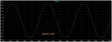
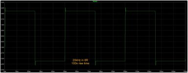
I’ll tell you a secret, maybe you didn’t know, a good transient response is important for an output stage that has switching distortion.I checked with Scope. The squarewave is perfect.
ECX10N20/ECX10P20 were developed as power transistors that do not have switching distortions, so a good square wave must be interpreted in a slightly different interpretation. for example, the effect of a capacitive load on the NFB at a point at the output of the amplifier.
Yeah, if the VAS current is high enough, then you can do without drivers for the mosfets.... Or you can apply enough feedback.I disagree. To say you need them simply isn't true. Look at Rod Elliott's P101. Simple approach with the VAS driving the lateral MOSFETs directly.
I agree that measured performance will improve. But the appeal of this design is its simplicity. It will be higher distortion, but the spectrum will likely be 2nd order dominate and monotonically descending. Look at the First Watt designs for inspiration. These don't measure well if low THD is your yardstick for performance. Yet they still appeal to many.
But I like a linear design without applying a lot of feedback. Have plenty of sims and measurement on actual hardware.... See this post:
https://www.diyaudio.com/community/...sfets-2sk3497-2sj618-a-little-testing.166301/
And you can't compare with First Watt, they all use Vertical mosfets, which don't have the same unlinear input capacitance problem that Lateral mosfet have, see the ciss curves in the datasheets....
You just have to be careful, as driving the output mosfets with low impedance emitter followers speeds them up....
All the chat. someone needs to build, measure and optimize this circuit! get the breadboards out guys 😎
I would, but I just built Lineup's Exiamp10 and now I've got the Cello One 15w ready for assembly.
Someone else needs to get on to this one!

@avtech
I am glad to hear you've built an amp designed by me. This is more than I expect
I am almost sure the Cello will work. Of course with small adjustments.
Good luck!
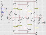
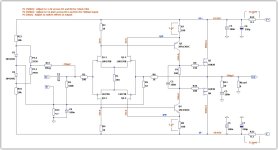
Now I have added Zobel filter at the output.
This will take care of 1uF capacitive loads.
Image shows the resulting amplifier.
I am glad to hear you've built an amp designed by me. This is more than I expect
I am almost sure the Cello will work. Of course with small adjustments.
Good luck!
Now I have added Zobel filter at the output.
This will take care of 1uF capacitive loads.
Image shows the resulting amplifier.
Attachments
You probably mean the option when a lot of feedback depth is distributed over separate amplification stages, i.e. the sum of local connections will be the total sum of negative feedback.But I like a linear design without applying a lot of feedback. Have plenty of sims and measurement on actual hardware....
This is a different way of forming linearity, which also has disadvantages. Linearity is directly proportional to the depth of feedback, regardless of whether it is local or general. The loss of the depth of the negative feedback of the variant with the sum of local ones is much more significant than with the general negative feedback. There are also disadvantages to General Negative Feedback. the best-sounding combination is still a combination of local and general negative feedback.
Having a highly unlinear capacitance involved have nothing to do with feedback.... It's just the influence of that capacitance can be reduced two ways, either by driving the capacitance with a low impedance source, or applying more negative feedback.... I don't like a lot of negative feedback, so I prefer the first choice, adding a couple of driver transistor it not really a big deal....
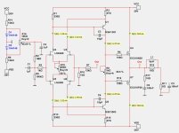
Here is how I would do it, simplied:
Here is how I would do it, simplied:
Attachments
Last edited:
deep local NFB)))Here is how I would do it, simplied:
I ran some sims with LSK170/LSJ74. This includes Hennady's suggestion to reroute the drains of Q1.2 & Q2.2. The feedback ratio was reduced to maintain gain and phase margin. I really like the clipping response. There's some overshoot on the square wave response, but not a lot of ringing.
Attachments
I ran the same sims using J113/J176. I got very similar results if the feedback ratio was increased by increasing R5 from 62 to 100. With J113/J176 the square wave overshoot was less and the 2MHz bump in the frequency response is gone. Distortion was a little bit higher.
I we pivot away from the matched LSK489/LSJ689 devices, seems like it would be worth providing provisions for LSK170/LSJ74 and J113/J176 on the PCB.
Any thoughts on this?
I we pivot away from the matched LSK489/LSJ689 devices, seems like it would be worth providing provisions for LSK170/LSJ74 and J113/J176 on the PCB.
Any thoughts on this?
I think you are not quite right.Running the JFETs are Idss. Still no pot connecting the sources. You would need to use matched LSK489/LSJ689 pairs. That makes this impractical to build in my opinion.
Nelson Pass has shown in amplifiers that you can run JFETs complementary 'at IDSS' without matching NFET and PFET.
But now I have added a sources resistance to JFETs.
This lower the currents in JFETs, but it does not change performance of the amp.
The THD is now 0.00047%
Attachments
I have been wrong many times
I think the challenge with running at Idss, is that the circuit becomes less predictable. I would think you would need to test it in sims are various Idss values to see it performs as expected. Look at my post #42. The currents through the different stage vary considerably with different Idss values. I would think you would want to avoid that.
I think the challenge with running at Idss, is that the circuit becomes less predictable. I would think you would need to test it in sims are various Idss values to see it performs as expected. Look at my post #42. The currents through the different stage vary considerably with different Idss values. I would think you would want to avoid that.
Using more common parts opens it up for more people can only be a good thing in my book. How about IRFP240/9240 outputs?
Exicon Lateral's are readily available from Profusion. Roughly £4 for laterals or £2 for verticals. So a £8 difference in price for the overall build.
- Home
- Amplifiers
- Solid State
- Ultra Amplifier with JFET input and Lateral MOSFET out