A bed time story --
") Here is an excerpt of what you might call an 'official' understanding of a CFA topology (Elantec) - The way it works; It is clear and concise. It could be helpful to someone trying to understand a CFA:
Here is an excerpt of what you might call an 'official' understanding of a CFA topology (Elantec) - The way it works; It is clear and concise. It could be helpful to someone trying to understand a CFA:
View attachment CFA Intersil.pdf
Apparently this EDN 1993 article is not found on the Internet (?).
Thx-RNMarsh
Here is an excerpt of what you might call an 'official' understanding of a CFA topology (Elantec) - The way it works; It is clear and concise. It could be helpful to someone trying to understand a CFA: View attachment CFA Intersil.pdf
Apparently this EDN 1993 article is not found on the Internet (?).
Thx-RNMarsh
Last edited:
Are-you sure ? I remember numbers a digit worse...But so many versions, witch one ? BIGBT ?I learn SSA from Lazy Cat. It give distortion figure better than VSSA
Vssa is something around 0.0004% at 50W 1kHz. And L.C. said Vssa sound better...
[edit]Ok, bimo, i see now your .asc, the cascoded version with BJT.
I've got 0.0003% (in sim) suppressing the capacitance at emitters of VSSA, moving the CSS to replace the collector 470 Ohm at 1.7mA, and adding shunt volt ref of - &+ 734mV from ground to the 47 ohms emitter to ground.
No more evil big lytic cap.
Last edited:
Are-you sure ? I remember numbers a digit worse...But so many versions, witch one ? BIGBT ?
Vssa is something around 0.0004% at 50W 1kHz. And L.C. said Vssa sound better...
[edit]Ok, bimo, i see now your .asc, the cascoded version with BJT.
I've got 0.0003% (in sim) suppressing the capacitance at emitters of VSSA, moving the CSS to replace the collector 470 Ohm at 1.7mA, and adding shunt volt ref of - &+ 734mV from ground to the 47 ohms emitter to ground.
No more evil big lytic cap.
Esperado, if you can make my circuit better in simulation, please share your asc file.
View attachment 376643
Apparently this EDN 1993 article is not found on the Internet (?).
Thx-RNMarsh
This I simulated using Elantec example.
I am not sure how good and simple this amp could be, but here is quick simulation. Very high slew rate but with some ringing.
BR Damir
Attachments
This I simulated using Elantec example.
I am not sure how good and simple this amp could be, but here is quick simulation. Very high slew rate but with some ringing.
BR Damir
CFA: A piece of cake, isn't it?
Now try using power FET, triple BJT OPS? Plot of power vs freq etc etc. Simple compensation scheme...
not a tapeze act to get phasing just so-so for stability and NFB for low HF distortion.
Thx-RNMarsh
Last edited:
125 W at a supply voltage of + -55 V, and 8 ohms
while reducing the load factor of 2 the output power is usually increased by 60 ... 80%, no more than
Petr
Hi Petr
Sorry for my late answer !
Yes I know that basic math ! , but what if we have reduced load factor for this specific CFA Amp by factor of 4 or even more ? , where associated Amp PSU is very powerfull & very stiff regulated ?
Regards !
Will try to sim-it. But said:Esperado thanks in advance ! , but regardless for some your minor mistakes I enjoy watching your work & contribution on this thread !
BTW , check this schematic too , it is about symmetric & GNFB free Amp with very interesting solution of VAS stage compensation .
Regards !
Attachments
CFA: A piece of cake, isn't it?
Now try using power FET, triple BJT OPS? Plot of power vs freq etc etc. Simple compensation scheme...
not a tapeze act to get phasing just so-so for stability and NFB for low HF distortion.
Thx-RNMarsh
That was triple BJT OPS I suppose.
Damir
This one was caricature. Something like traveling in plane...without any plane ;-).but regardless for some your minor mistakes
Thanks, anyway for your kind words (non merited).
I don't feel comfortable with sims, it is too far from reality, we need to listen and compare the things we are working on. Simulating only is like painting with a blindfold.
Look what happens in this thread: some very complex designs, with low numbers, some very simple ones, 5X worse numbers. How can-we get an experience on this if we don't compare the sonics ?
To give an example, diamonds sims very well. Each time i had tried them in a VFA, i was disappointed by the sonic. And it seems, if i remember well, that L.C. shared the same experience. Of course, pure objectivists will disagree.
Same thing with Jfets input in CFAs: it can solve some DC and phase problems, it sound warm, little details lost in the sonic.
From you first schematic, it is very close to my personal amp, VAS cascoded.
I would try to simplify.
Dadod, can-you smell-it ?
About your second picture, i don't understand: no feedback from OPS ?
I have designed and modified various CFB amps ( and preamps). My religion as a start, now, is very simple: Lateral in OPS (i have no experience with IGBT), BJT in input, and as simple as possible: simpler the signal path, better it sound, despite the distortion numbers.
I had tried quickly your second schematic idea: i see no advantage, like each time i had tried multiple feedbacks.
Well, sims have at least an advantage: never a smoke or a smell of burnt
That was triple BJT OPS I suppose.
Damir
I mean - try both types in OPS. and compare.... in my example of real live circuit performance (not sim) it had MOSFET outputs and very low THD even at full power/freq.
-Richard M.
Last edited:
I've got 0.0003% (in sim) suppressing the capacitance at emitters of VSSA, moving the CSS to replace the collector 470 Ohm at 1.7mA, and adding shunt volt ref of - &+ 734mV from ground to the 47 ohms emitter to ground.
No more evil big lytic cap.
I had asked LC to do same in his circuit to bring topology up-to-date.
-RNM
Resume:
In The VSSA, LC had set a current source for each symmetrical branch, emitter side.
The problem is gain is lost in the input stage, cause emitter resistance +CCS impedance is higher than the collector resistance. He solved-it by a big capacitor to ground at the css/resistance emitter point. With the inconvenience that this cap is very high value, because the emitter resistance is low. With added distortion at low frequencies, due to phases errors, and group delay error.
So, i tried to set this CCS, collector side, replacing the collector resistance.
And, emitter side, a voltage reference (shunt regulator ?).
Surprisingly, it even reduce a little distortion and work very well. I wait for my VSSA to try and compare.
Attachments
Last edited:
Resume:
In The VSSA, LC had set a current source for each symmetrical branch, emitter side.
The problem is gain is lost in the input stage, cause emitter resistance +CCS impedance is higher than the collector resistance. He solved-it by a big capacitor to ground at the css/resistance emitter point. With the inconvenience that this cap is very high value, because the emitter resistance is low. With added distortion at low frequencies, due to phases errors, and group delay error.
So, i tried to set this CCS, collector side, replacing the collector resistance.
And, emitter side, a voltage reference (shunt regulator ?).
Surprisingly, it even reduce a little distortion and work very well. I wait for my VSSA to try and compare.
Esperado, you did not eliminate big electrolytic caps, just replaced them with ideal low voltage source. In LC design big electrolytic caps are in the feedback path and they provide low impedance to the ground. To construct a shunt regulator, as you suggest, with so low voltage and low output impedance is almost impossible, so electrolytic caps are much more elegant solution, but not the best. You don’t read Self, but he shows that the electrolytic cap in the in the feedback part should be of much higher capacitance then LF corner calculation shows, due to higher distortion at low frequencies. Better without those caps if could be designed.
BR Damir
I mean - try both types in OPS. and compare.... in my example of real live circuit performance (not sim) it had MOSFET outputs and very low THD even at full power/freq.
-Richard M.
Problem is that simulation will not show close to real distortion with mosfets OPS as the models I have are not accurate enough and I can't find the better ones.
BR Damir
The problem is now very different. In the original schematic, the cap is requested (infinite impedance at DC) to let the current source biasing the transistor. Now, we just need some voltage reference, (0 to infinite). With 0.2V of dynamic impedance, i believe some TL431 will work perfect with the help of a little film cap at HF. We only ask this voltage reference to be linear in frequency.Esperado, you did not eliminate big electrolytic caps, just replaced them with ideal low voltage source.
So obvious.The cap introduce phase shift, thus reduce the error correction accordingly. Well, i asked the question about the way supercaps sounded, here, but had no answer.You don’t read Self, but he shows that the electrolytic cap in the in the feedback part should be of much higher capacitance then LF corner calculation shows, due to higher distortion at low frequencies.
Last edited:
I had asked LC to do same in his circuit to bring topology up-to-date.
-RNM
I have done this - very easy to do. I may post up the concept diagram in the next few days.
I had asked LC to do same in his circuit to bring topology up-to-date.
-RNM
That is to say, I said to LC to make same changes I did in 1980-ish to eliminate all audio signal carrying electrolytic capacitors. You (and LC) really need to get rid of electro-cap in circuit. Then, it will perform and sound even better. [plus smaller pcb size circuit, lower BOM cost and greater reliability - if any of that matters] .
Thx-RNMarsh
Last edited:
...Firstly, the SMALLER the loop, the more stable its likely to be....
A smaller, simpler loop is also less likely to have evil parasitics cos your layout can be simpler & tighter .. and hence will be stable with a higher ULGF.
Yes, of course. But most of the excess phase will be from the slow outputs and drivers so I would be surprised if the omission of just the comparatively fast IPS means you can safely quadruple the ULGF.
BTW, Cherry's ETI apr83 article is on Jan.didden's website
Thanks, I already have that, plus the JAES articles in hard copy, and the November 192 ETI article, but I appreciate the reminder.
A Locanthi triple, QUAD triple, 'EF2+single VAS' (all 'Inner Loops' including the Locanthi triple EF) with MJ3281/1302 all have a Current gain ULGF much higher than 30MHz.
ULGF is the same for current or potential because LG is the same for both.
I prefer to use the term Return Ratio, to emphasis that it is dimensionless.
But Current gain, though appropriate to work out how much they contribute to the overall Loop Gain, isn't the right metric to judge the stability of the 'Inner Loops'.
The key to stability in all 3 cases is reducing the Gm of the 'inner loop'.
Since Return Ratio is dimensionless I don't really understand your point.
The probe at the IPS shows stability of the whole amp. You need to look at both.
You absolutely need to look at both.
At the risk of generalising, IMHO, the IPS probe is the more important one. The 'inner loop' is just one of the blocks within the 'main loop'. The 'main loop' inherits all the evil very HF poles of the 'inner loop' but if these are relatively even higher for the 'main loop', they are innocuous.
Either I misunderstand your point or I think you are mistaken.
An amp can have an unstable inner loop, this is does not have to make the outer loop unstable.
Consequently the outer loop stability indicators will look fine.
For the .ASC I posted in #1480, reducing C1/3 reduces LG for the 'inner' Cherry loop (ie makes it more stable) but increases it for the main 'IPS' loop. This reduces the stability of the complete amp...
Yes, different capacitors just move the gain between the inner and outer loop so don't really help.
That's why people fall back on various forms of shunt compensation.
This is a valid technique but no more useful than increasing one of the 'more' dominant poles within the loop or trying various capacitive loads. IMHO, the last is the most useful cos it ties in with important 'real life' tests which you need to do.
Different capacitive loads is an excellent test.
But I suspect that if the OPS is well buffered then the different loads may not impact the inner loop(s) much.
A time delay will always impact the inner loop(s) so should be a more robust test.
But I haven't actually tested the tests, do you have any data on this?
If this is astx's supa amp, you'll remember we couldn't sim his stability results either.
But we both had identical conditions.
The limitation of the model is not an excuse.
All models are limited so tolerance of model inaccuracies is useful in itself.
But more importantly, it usually also reflects tolerance of real world imperfections.
And the OIC did worse in both aspects.
I think the point about making the 'inner Cherry loop' more stable reduces the stability of the complete amp is the relevant one. It is borne out in 'real life'.
Yes, if you try to stabilise the Cherry loop with variation of the capacitor value.
Best wishes
David
Last edited:
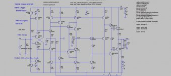
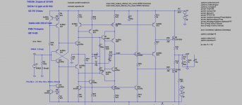
Lateral MOSFET OPS.
This one is with a strange compensation and it's very stable even up to 200 nF without output inductor. With all my lateral mosfer OPS distortion is much higher if OPS is not included in compensation circle, even if it is distortion at 20 kHz is not something to write home about.
I am not sure if those distortion result are any close to real life amp.
I those last two CFA amp I am back to the current conveyor used in my GainWire pre amp, just in this case it's diamond but not with Baxandall pairs. No big difference in both cases.
BR Damir
Attachments
- Home
- Amplifiers
- Solid State
- CFA Topology Audio Amplifiers