Hi,
As I am happy with V3 pcb AD1862 two layers board from Miro with a OP1655 as a to do all operational amplifier, I wanted to go further. Inspired by his work I wondered about what I wanted to add and what I wanted to give up as a trade off consequence. Cost ? Size ? Complexity ? Maybe wasted monney ? Mostly this is definitly a keeper dac chips with the TDA1541 I have already from Pedja Rogic with personal mods, some of them were published in Aya 2 from 2014 to Aya 4 manuals on an other diyer name of mine.
I had a gross envy to try the discrete Mosfet D1 I/V from path, sligthy modified by our migthy ZM (@Zen Mod ) . It has some very wanted feature for I/V stage : very low input current noise of Fet family chips while here it's a Mosfet, a very low input impedance as the curent based operational amplifier but w/o that 1K Z input resistor (you know the Johnson noise and resistor coloration when going higher than a couple of hundred Z; and its stray capacitance or inductance). I either didn't wanted to go for the mess of discrete matched parts and complementary as well as a too much big discrete layout to see if one could profit of Heny Ott, Archeambault, etc, EMI/EMC layout practices to try very fast, very precise, high bandwith, operationals amplifiers for the I/V task. I played also with power line length for inductance as a wanted trade off around the operationnal amplifiers.
Also wanted a a second stage with different quality as a buffer for headphones and usual capacitive loads. Two operationnal amplifiers add in complexity but not so much and give a lot of versatility to choose the good ones for each task to balance the sound one is looking for. And the dedicate power supply of the output stages permits to play with different Vdc than the 12Vdc needed for the "analog" section of the AD1862, though I treated in my layout the digital PS of the dac chips as an analog ground to only manage a digital ground for the digital signals. And yes of course they "see"" each others.
In spite of two layers with a 1.5 mm core between the two layers, the 4 layers permitted to put the second layer and main ground (well they all communicates but where it counts 🙂 )at only 6 miles (0.15 mm) to make possible better decoupling due to the high speed of the operationnal amplifiers I chose. Also it's better for the ground loops and so, capacitors inductances for the high frequencies decoupling (no leads)...
Mainly as I like a lot to play with passive parts too, the goal was the two chips do not share the same local capacitors and decoupling and have a separate power supply from the DAC chips. I greatly whished a 4 layers pcb for a finer routing, current ground loops, striplines impedance, stray capacitance, power supply, management and something different in the digital and analog ground section. So I totally re designed miro1360 pcb, sacrificing the low cost, almost through hole parts philosophy and universality (a pcb made for almost all, beginners included). The internal layers and routing design took me more a hundred on hours on 2 months to refine. I also gave up the pots elements matching that brings nothing really important for the ears as said miro1360. It is too much hard to make okay without scope and suffers from the pots precision and drift; I would add the traces coupling makes antennas too between tacks and between dac chip pins.
So was it worthing the journey ? Well it's a hobby, it is more expensive to print,a power supply more. And yes some blend of aops are worthing it; you know some have swapped SK170 discrete parts from some operationnal amplifiers for the input stage of some Pass amps with better sonic results. All is not about very low noise but also about layout. You know already some guys like Pedja Rogic or Thorsten Loesch do not design their DAC with ultra very low noise to sacrifice other wanted features... It's a whole. I tried to apply what I learned from all the members and also wanted to give something, so I designed a cheaper 2 layers boards for the community with the main good features if some want to experiment with the oaps of their choices (no BOM nore support from me).
The two layers board is the JLSOUNDS and uf-l pads stack version of miro1360 with just the redesigned two aops stage and its own power pins. It is including some nice features of the 4 layers I have: 1/5 distance inch between the AD1862 output and the inverting pin of the i/v OP for better inductance (short is what is important here), the stray capacitance layout is enhanced. As a consequence, the lythic caps are only 7 mm diameter allowed and pins pitch is 2.5 mm. The smd decoupling caps are "only" 0805 casing (made for the acrylic 0.1uF/16V caps, fromCDE). SMD resistor are 1208 casing and MELF resistor not advised due to their inductance behavior (though I like A LOT the carbon made MELF for both I/V and coupling here), better thin film SMD Vishay (<= 1/4 W 1% precision are enough). In mine I soldered the I/V resistor on the side, the pad is ok to add a decoupling capacitor (ceramic NPO 20 pF in mine). There is a resistor between the OPs to damp output and input of the next stage (tip 50R is okay wiyh most and only NanoV noise, also ok at the output (Alen Bradley carbon comp 1/-4 or 1/8W are great. With mine I used a G+2 and with the 50 R output resistor that is greatly advised, it forms a G+1 buffer stage. So indeed the second OP is a voltage follower using at the input the non inverting input. The cans lovers migth choose some nice ops for their needs BUF04 or else. Two channels and four OPs are feeding from a standalone power supply header, so choose the voltages your opas work better with.
Two layers, it is staying cheap as I bet the few whom will try have already several boards and it is not made for people w/o smd soldering experience nore beginners as there is no BOM. Though I advice Panasonic caps for OPs, APSA polymer cap for the digital section of the AD1862 (Pan FR here is also a great choice) and for the two filter decoupling caps of the AD1862, the Nichicon UKL is a great choice orPan FR (but beware of the little space and pins pitch : mounting some from the back is adviced.) Anyway your choice as it's a niche pcb ! Do feed the AD1862 5v and 12v with miro PCBs 2 you just have to solder a 3 wires more on the 12V output cause I had to split the 12V feeding of the dac chips with two headers. And yes the pcb is the same size from the great Miro board from which I worked on (my 4 layers is bigger as the routing front is also different).
And Ah (ah), I had to give a stupid ego centred name to my 4 layers PCB. Called it The Extinction DR* edition DAC : one DAC to end them all (of course it is not true, but still better sounding than many low cost DACs made Sigma Delta). Note : *: DR = Deaf Rooster... well I'm french but hesitated with DF for frog ! I would name the two layers : "have pleasure with it, it is good enough" and you have something concrete to play with after the effort of the long blah reading 😁. The two layers was not tested, but no DRC errors, if vias errors due to the through holes restriction of JLPCB, let me know I correct the gerbers (but very rare with a 2 layers design), but I have tripled checked and my 4 layers on which it is based sound eveyday. Is it better than the finest assemblies here, I dunno, don't ask; better to call Saul. If one or two people uses it, it has worth the time I spent.")
cheers, diyiggy
Is a step file is ok enough for printing? Green is the two layers. Blue is the 4 layers with different digital streamer PS options.
As I am happy with V3 pcb AD1862 two layers board from Miro with a OP1655 as a to do all operational amplifier, I wanted to go further. Inspired by his work I wondered about what I wanted to add and what I wanted to give up as a trade off consequence. Cost ? Size ? Complexity ? Maybe wasted monney ? Mostly this is definitly a keeper dac chips with the TDA1541 I have already from Pedja Rogic with personal mods, some of them were published in Aya 2 from 2014 to Aya 4 manuals on an other diyer name of mine.
I had a gross envy to try the discrete Mosfet D1 I/V from path, sligthy modified by our migthy ZM (@Zen Mod ) . It has some very wanted feature for I/V stage : very low input current noise of Fet family chips while here it's a Mosfet, a very low input impedance as the curent based operational amplifier but w/o that 1K Z input resistor (you know the Johnson noise and resistor coloration when going higher than a couple of hundred Z; and its stray capacitance or inductance). I either didn't wanted to go for the mess of discrete matched parts and complementary as well as a too much big discrete layout to see if one could profit of Heny Ott, Archeambault, etc, EMI/EMC layout practices to try very fast, very precise, high bandwith, operationals amplifiers for the I/V task. I played also with power line length for inductance as a wanted trade off around the operationnal amplifiers.
Also wanted a a second stage with different quality as a buffer for headphones and usual capacitive loads. Two operationnal amplifiers add in complexity but not so much and give a lot of versatility to choose the good ones for each task to balance the sound one is looking for. And the dedicate power supply of the output stages permits to play with different Vdc than the 12Vdc needed for the "analog" section of the AD1862, though I treated in my layout the digital PS of the dac chips as an analog ground to only manage a digital ground for the digital signals. And yes of course they "see"" each others.
In spite of two layers with a 1.5 mm core between the two layers, the 4 layers permitted to put the second layer and main ground (well they all communicates but where it counts 🙂 )at only 6 miles (0.15 mm) to make possible better decoupling due to the high speed of the operationnal amplifiers I chose. Also it's better for the ground loops and so, capacitors inductances for the high frequencies decoupling (no leads)...
Mainly as I like a lot to play with passive parts too, the goal was the two chips do not share the same local capacitors and decoupling and have a separate power supply from the DAC chips. I greatly whished a 4 layers pcb for a finer routing, current ground loops, striplines impedance, stray capacitance, power supply, management and something different in the digital and analog ground section. So I totally re designed miro1360 pcb, sacrificing the low cost, almost through hole parts philosophy and universality (a pcb made for almost all, beginners included). The internal layers and routing design took me more a hundred on hours on 2 months to refine. I also gave up the pots elements matching that brings nothing really important for the ears as said miro1360. It is too much hard to make okay without scope and suffers from the pots precision and drift; I would add the traces coupling makes antennas too between tacks and between dac chip pins.
So was it worthing the journey ? Well it's a hobby, it is more expensive to print,a power supply more. And yes some blend of aops are worthing it; you know some have swapped SK170 discrete parts from some operationnal amplifiers for the input stage of some Pass amps with better sonic results. All is not about very low noise but also about layout. You know already some guys like Pedja Rogic or Thorsten Loesch do not design their DAC with ultra very low noise to sacrifice other wanted features... It's a whole. I tried to apply what I learned from all the members and also wanted to give something, so I designed a cheaper 2 layers boards for the community with the main good features if some want to experiment with the oaps of their choices (no BOM nore support from me).
The two layers board is the JLSOUNDS and uf-l pads stack version of miro1360 with just the redesigned two aops stage and its own power pins. It is including some nice features of the 4 layers I have: 1/5 distance inch between the AD1862 output and the inverting pin of the i/v OP for better inductance (short is what is important here), the stray capacitance layout is enhanced. As a consequence, the lythic caps are only 7 mm diameter allowed and pins pitch is 2.5 mm. The smd decoupling caps are "only" 0805 casing (made for the acrylic 0.1uF/16V caps, fromCDE). SMD resistor are 1208 casing and MELF resistor not advised due to their inductance behavior (though I like A LOT the carbon made MELF for both I/V and coupling here), better thin film SMD Vishay (<= 1/4 W 1% precision are enough). In mine I soldered the I/V resistor on the side, the pad is ok to add a decoupling capacitor (ceramic NPO 20 pF in mine). There is a resistor between the OPs to damp output and input of the next stage (tip 50R is okay wiyh most and only NanoV noise, also ok at the output (Alen Bradley carbon comp 1/-4 or 1/8W are great. With mine I used a G+2 and with the 50 R output resistor that is greatly advised, it forms a G+1 buffer stage. So indeed the second OP is a voltage follower using at the input the non inverting input. The cans lovers migth choose some nice ops for their needs BUF04 or else. Two channels and four OPs are feeding from a standalone power supply header, so choose the voltages your opas work better with.
Two layers, it is staying cheap as I bet the few whom will try have already several boards and it is not made for people w/o smd soldering experience nore beginners as there is no BOM. Though I advice Panasonic caps for OPs, APSA polymer cap for the digital section of the AD1862 (Pan FR here is also a great choice) and for the two filter decoupling caps of the AD1862, the Nichicon UKL is a great choice orPan FR (but beware of the little space and pins pitch : mounting some from the back is adviced.) Anyway your choice as it's a niche pcb ! Do feed the AD1862 5v and 12v with miro PCBs 2 you just have to solder a 3 wires more on the 12V output cause I had to split the 12V feeding of the dac chips with two headers. And yes the pcb is the same size from the great Miro board from which I worked on (my 4 layers is bigger as the routing front is also different).
And Ah (ah), I had to give a stupid ego centred name to my 4 layers PCB. Called it The Extinction DR* edition DAC : one DAC to end them all (of course it is not true, but still better sounding than many low cost DACs made Sigma Delta). Note : *: DR = Deaf Rooster... well I'm french but hesitated with DF for frog ! I would name the two layers : "have pleasure with it, it is good enough" and you have something concrete to play with after the effort of the long blah reading 😁. The two layers was not tested, but no DRC errors, if vias errors due to the through holes restriction of JLPCB, let me know I correct the gerbers (but very rare with a 2 layers design), but I have tripled checked and my 4 layers on which it is based sound eveyday. Is it better than the finest assemblies here, I dunno, don't ask; better to call Saul. If one or two people uses it, it has worth the time I spent.
cheers, diyiggy
Is a step file is ok enough for printing? Green is the two layers. Blue is the 4 layers with different digital streamer PS options.
Attachments
-
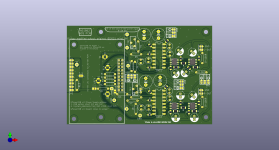 diyAudio_AD1862_DAC_v1.3_uf.l_jlsounds-notFlipped - Diyiggy modifications.png99.8 KB · Views: 92
 -
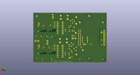 diyAudio_AD1862_DAC_v1.3_uf.l_jlsounds-notFlipped - Diyiggy modified (back).png50.2 KB · Views: 105
 -
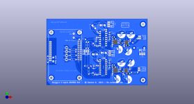 DIYIGGY Extinction DAC.png73.6 KB · Views: 92
 -
 chicken head.jpg22 KB · Views: 100
 -
diyAudio_AD1862_DAC_v1.3_uf.l_jlsounds-notFlipped. Diyiggy modification.step773.9 KB · Views: 28
Last edited:
Notice : I add to check if the OPs foot prints are ok as the first one is larger (it is just the pads pitch for better routing bellow the OP for the I/V one), but the current pads print is the one of the buffer which looks smaller OP in the picture. Let me know if you want to know the size of each.
Notice : forget it, I was talking for the 4 layers; 2 layers are standard OP smd foot prints for both OPs.
Notice : forget it, I was talking for the 4 layers; 2 layers are standard OP smd foot prints for both OPs.
Attachments
Last edited:
A fumbling use of the search tool has yet to uncover v3 of Miro's board. Link anyone?As I am happy with V3 pcb AD1862 two layers board from Miro
Regards,
Dan
If you havent seen this link on post 1, its super helpful for navigating the 400 pages of posts here.
https://electrodac.blogspot.com/p/dac-ad1862-almost-tht-i2s-input-nos-r.html
https://electrodac.blogspot.com/p/dac-ad1862-almost-tht-i2s-input-nos-r.html
Excellent suggestion. Just recently I noticed this project and I'm catching up on four years of posts. Short term, I'm building the recommended power supplies and searching for some AD1862s.If you havent seen this link on post 1, its super helpful for navigating the 400 pages of posts here.
https://electrodac.blogspot.com/p/dac-ad1862-almost-tht-i2s-input-nos-r.html
Regards,
Dan
Tubes are the way to go. Try better capacitors or put transformers at the output.Wired, powered on...
It is leading me to tears 😭😭😭
Never heard my system sounding with this delicacy, finesse, depth, precision, it's something I can't describe with few words...
Miro, Grunf, you're the GOATs!!!! (Pardon Grunf, perhaps Miro a little more in this particular case)
It's moving.
È commovente, ho i brividi, non vorrei mai fermarmi di ascoltare, è una roba incredibile, tonight I could pass on football Italy -Albania to listen to this...
So Rehan, here how it looks like on the three inputs:LRCLK is to taken from "output" of switching board. Now each board (if I remember right) has 3 LEDs, whichever input is selected the corresponding LED will turn on, and that is "High" status, you can choose either not to solder LEDs and connect those wires to Arduino or connect the LED and solder the wires from Arduino to switching board LED pins.
Personally I found the idea of connecting too many board cumbersome, thus I chose an AK4118 board which gives me all these option.
Things are,
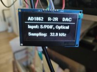
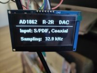
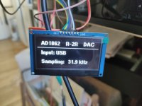
-shown sample remains at 33khz, I put a 96khz file in, it showed very briefly 100khz and turned again on 33khz.
-input shown dances in-between the two states USB/coax or coax/optical, I touch the pin with my multimeter, it turns correct. For this I think I need some shielded cable, now I'm using the first I had at hand.
Code is attached.
Attachments
I haven't gone through the whole code thoroughly but apparently you are using analog read, change it to digital read (connect to digital pins), I think one of the analog pin is floating.
Nice work though.
Also I think I mentioned earlier that the display that you have, although it is SPI right now but if you change a resistor at the backside of PCB it would become an I2C display thus instead of 7 pin SPI interface you' ll need only two signal lines (SDA,SCL).
Nice work though.
Also I think I mentioned earlier that the display that you have, although it is SPI right now but if you change a resistor at the backside of PCB it would become an I2C display thus instead of 7 pin SPI interface you' ll need only two signal lines (SDA,SCL).
Last edited:
Thanks @rehanabid, I guess I'll need more time to finalize that.
And also scope for 5 seconds the lrclk pin in the DAC board.
I need to figure out how to output the live Arduino code, so I can get an idea and solve.
Now that I've SPI I don't want i2c anymore, I've got the start animation 😁
And also scope for 5 seconds the lrclk pin in the DAC board.
I need to figure out how to output the live Arduino code, so I can get an idea and solve.
Now that I've SPI I don't want i2c anymore, I've got the start animation 😁
one of the drawbacks I found about the sample rate display this one and the commercial ones is that they don't refresh the sample rate often, e.g; the first song you played was 16 bit/44.1Khz and the next one is 24bit/96Khz you are most likely to get the sames 44.1Khz sample rate. I added another sub-function to check the sample rate very 30 seconds and then refresh the display.
You can use it if you want.
Excellent progress on the DAC, I might (in the future) consider using your tube IV stage once I am done with "Mr. V's" IV stage.
// Check if 30 seconds have passed since the last display update
if (currentMillis - previousMillis >= updateInterval) {
previousMillis = currentMillis;
checkAndUpdateSampleRate();
}
You can use it if you want.
Excellent progress on the DAC, I might (in the future) consider using your tube IV stage once I am done with "Mr. V's" IV stage.
That's already in use, wanted to ask if there is some drawback on setting the updateinterval to 5 seconds?
yes, consider the tube stage, the sound envelopes you like in a magic ball, you can't do anything else than listening with your heart high and with full mind... I guess this is perhaps the best sounding piece of equipment i ever built, and they are not few...
yes, consider the tube stage, the sound envelopes you like in a magic ball, you can't do anything else than listening with your heart high and with full mind... I guess this is perhaps the best sounding piece of equipment i ever built, and they are not few...
@rehanabid and @Michelag : on the tube pcb, in your shoes, I would consider to solder the resistors pins on the tube side even shorter to avoid oscillation. (the resistors layout in the opa stages is also layouted for that in my pcb as well as for lowest inductance )
Can be made w/o mod the pcb. Just solder the lead of the resistor on the tube side directly on the tube socket pins in spite of the resistor vias. 4 mm from the resistor body to the tube pin. No longer.
I also use a Mu follower with a E188CC which is a low noise long life, 5% matched half triode pair from the plant, enhanced E88CC with Moglia circuitry inspired from @gaszto in this thread that shared. But for a TDA1541 made DAC. Once a day a friend from Australia explain me well the magic of T Loesch idea : the negative compliance output of the TDA1541A curent output is perfect to attack a tube grid (negative ). He added with this dac chip then, no one should use a biased to ground typology as Marvelaudio site talked, but that is another story that doesn't bellong to this thread. The AD1862 has the digital zero drifting between +1 & -1 mA if my memory serves me well. Possible but less effective. Asking greater Mu to be confortable. Greaterr Mu than the 33 of ECC88 asks care about oscilllation (remember 3DA) too and anyway a capacitor output DC blocker (or an OT but in this case what you hear is more the trafo than the tube... trade off trade off) !
The low fet is a J113 in spite of the less quiet J310. J113 has often around 15 mA output which is perfect with the 17 mA output of the ECC88 family. Make them working in a close push pull operation near SRPP topology. The power Mosfet at upper position is of course a high voltage depletation Mosfet from IXTP.
Grunf shematic is nice too. The tube is what is making the greatest difference. If using the soviet tube Michelag talked, choose indeed only the EV version and before 1980 made. I have the envelopp too with operationnal amplifiers ! In the blog from Miro (first page of this thread for link) you will find a Thorsten Loesh paper link for I/V tube I and Grunf copied the pdf in this thread. (mine was the further revised paper on which the link is)
)Can be made w/o mod the pcb. Just solder the lead of the resistor on the tube side directly on the tube socket pins in spite of the resistor vias. 4 mm from the resistor body to the tube pin. No longer.
I also use a Mu follower with a E188CC which is a low noise long life, 5% matched half triode pair from the plant, enhanced E88CC with Moglia circuitry inspired from @gaszto in this thread that shared. But for a TDA1541 made DAC. Once a day a friend from Australia explain me well the magic of T Loesch idea : the negative compliance output of the TDA1541A curent output is perfect to attack a tube grid (negative
). He added with this dac chip then, no one should use a biased to ground typology as Marvelaudio site talked, but that is another story that doesn't bellong to this thread. The AD1862 has the digital zero drifting between +1 & -1 mA if my memory serves me well. Possible but less effective. Asking greater Mu to be confortable. Greaterr Mu than the 33 of ECC88 asks care about oscilllation (remember 3DA) too and anyway a capacitor output DC blocker (or an OT but in this case what you hear is more the trafo than the tube... trade off trade off) !The low fet is a J113 in spite of the less quiet J310. J113 has often around 15 mA output which is perfect with the 17 mA output of the ECC88 family. Make them working in a close push pull operation near SRPP topology. The power Mosfet at upper position is of course a high voltage depletation Mosfet from IXTP.
Grunf shematic is nice too. The tube is what is making the greatest difference. If using the soviet tube Michelag talked, choose indeed only the EV version and before 1980 made. I have the envelopp too with operationnal amplifiers
! In the blog from Miro (first page of this thread for link) you will find a Thorsten Loesh paper link for I/V tube I and Grunf copied the pdf in this thread. (mine was the further revised paper on which the link is)
Last edited:
@Michelag Is that USB with this board? https://www.diyaudio.com/community/...s-input-nos-r-2r.354078/page-113#post-6702510
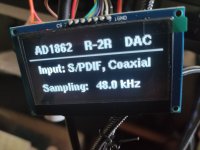
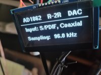
USB in this board can do max. 48kHz, it is the limitation of PCM2706. If you put the signal with Optical or SPDIF, it can make 96.
96 and more from USB can be obtained with devices based on XMOS, atmel, STM32, ...
USB in this board can do max. 48kHz, it is the limitation of PCM2706. If you put the signal with Optical or SPDIF, it can make 96.
96 and more from USB can be obtained with devices based on XMOS, atmel, STM32, ...
@miro, in that moment I was using optical.
Yes, I've got that board, but I'm using raspberry with Moode on USB... Still didn't try lrclk on USB...
Perhaps something wrong in the shift register? How do I get 96khz there?
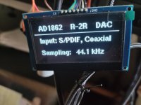
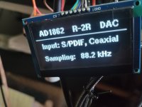
Tested coax, 44, 96, it's working. Don't have any 192 to test with 🤔
Yes, I've got that board, but I'm using raspberry with Moode on USB... Still didn't try lrclk on USB...
Perhaps something wrong in the shift register? How do I get 96khz there?
Tested coax, 44, 96, it's working. Don't have any 192 to test with 🤔
Last edited:
Ok, sorted things out.
Now I would need some model of USB boards with xmos, atmel, amanero that don't cost more than 50€ 😉 (that jbboard costs alottofmani)
And perhaps figure out a way to get both SPDIF (coax and opt) up to 192khz. We would need some chip that does that... I don't know if there's one on the market, and if its implementation on the actual board is easy.
For the moment I'm happy. 😁
Oh yes I need some sort of enclosure...
Every time I listen to it, independently from the kind of music, I can't help but having a 30s brain freeze, how good it sounds!!! 😁😁😁
Attachments
- Home
- Source & Line
- Digital Line Level
- DAC AD1862: Almost THT, I2S input, NOS, R-2R