@baggerbole Try different USB cable, different USB slot, different computer if is that possible.
If nothing from above helped, power up the jlsounds board by method 3 (in manual on the page 3)")
If nothing from above helped, power up the jlsounds board by method 3 (in manual on the page 3)
From what I remember is that JLSound has an SPDIF out function as well, what I will be doing in your position is as follows:Thanks Miro.
But it doesn´t play music
1) get the SPDIF function working, separate the JLSound from the DAC and play some music via usb, get the SPDIF out and put it to any other amp, if there is sound then it means the JLSound I2S is working.
2)In my experience crackling noise through DAC is only produced when the digital inputs are incomplete mean one of the signals is missing LRCK, BCK or Data.
I think I experienced the same in one out of the three DACs that I made earlier, turned out there were two problems in one case the shift register got over heated during soldering and was was gone, second time there was problem at the connector.
One has to check output at each shift register.
@miro1360
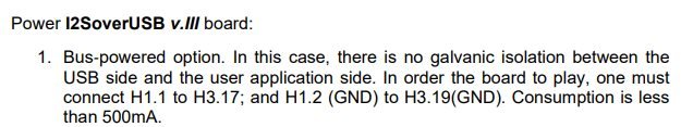
Power supply is connected according to manual page 3
@rehanabid
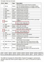
I don´t use the shift register as Miro recommended(see pic). DATA is splitted in DL and DR on JL I2S board and connected to DAC board.
I don´t have an amp with SPDIF in...
Power supply is connected according to manual page 3
@rehanabid
I don´t use the shift register as Miro recommended(see pic). DATA is splitted in DL and DR on JL I2S board and connected to DAC board.
I don´t have an amp with SPDIF in...
Attachments
Here are also Gerbers and schematics for the D1 thanks to the mighty ZM.
The D1 featured a PCM63, spec sheet says output for that chip is +/- 2ma - the AD1862 outputs +/- 1ma. I am not qualified to comment on what result that would have in the circuit but hopefully that is in some way helpful to you
The D1 featured a PCM63, spec sheet says output for that chip is +/- 2ma - the AD1862 outputs +/- 1ma. I am not qualified to comment on what result that would have in the circuit but hopefully that is in some way helpful to you
Last edited:
It means that the I/V circuit will produce half the output voltage amplitude/gain via the AD1862, but also decreased distortion as a result of that. The decreased gain can be compensated for if required, but doing so would then have the consequence of altering both MOSFET's bias conditions. Likely resulting in increased distortion.Here are also Gerbers and schematics for the D1 thanks to the mighty ZM.
The D1 featured a PCM63, spec sheet says output for that chip is +/- 2ma - the AD1862 outputs +/- 1ma. I am not qualified to comment on what result that would have in the circuit but hopefully that is in some way helpful to you
Last edited:
The square waves are not very clean?@miro: As on Vunce´s I2S board there is no U10 installed. It looks like a layout design revision.
The jlsounds doc describes B1 to B5 short bridges. On my board it´s B1 to B6 as you can see from first picture in post #3245.
@woodturner-fran: Yellow trace is lrck, blue is bck (first screen shot)
Yellow trace = DL, Blue trace = DR (third screen shot)
LRCK should be 64xBCK slower Try different USB cable (shorter) because it must deliver 400mA
That makes sense even to me but I would have no clue how to change that....and I'm not asking for a solution here dont worry.!It means that the I/V circuit will produce half the output voltage amplitude/gain via the AD1862,
Gives me some homework to do.
Maybe I just turn the volume up some more or use with a higher gain pre amp.?!
@jimk04 - undoubtedly there will be an IV resistor that you need to size to suit the DAC chip. Also some chips might have a DC offset that you need to take care of, I think the 1541 has that.
I have one of the Spencer Pass D1 dacs from years ago - very nice sounding bit of kit.
I have one of the Spencer Pass D1 dacs from years ago - very nice sounding bit of kit.
Baggerbole I hope you soon get this sorted.
I'm planning some 'next moves 'and have the Euvl and Pass D1 IVs to build up.
Does anyone know if the D1 as per Pass schematic is suitable as is for the AD1862. I got some D1 boards spare if anyone wants.
It is suitable. Which schematic do you use? Simple change in resistor can increase the output voltage per mA input
The green power LED on JLsound board is shining bright and the heat sink is hot.
I assume no power problem.
If LRCK is 64 times too fast it must be a configuration error.
I ask at JLsounds for a solution.
I hope you will find the solution soon. Because you are so close to nice sounding DAC

How many digital inputs can be measured by your scope?
This is the one I have and also used the gerbers linked someway back to have some boards made.Which schematic do you use?
EDIT: scratch the following comment, the jumpers for AD1862 12v are arranged in such a way that I can use the molex connectors for those and the regular 12v for my analog stage. Perfect!Hi Jim,
These are the Molex KK series headers, crimps and connectors that all mate together plus the Engineer PA 20 crimper pliers for perfect crimp jobs. 👍
https://www.mouser.com/ProductDetail/Molex/22-01-3027?qs=cRUT3GdJqnwywyFd19%2BSsA==
https://www.mouser.com/ProductDetail/Molex/22-23-2021?qs=ILqg114nvd4YKlRlbo3yMg==
[URL
unfurl="true"]https://www.mouser.com/ProductDetail/Molex/22-01-3027?qs=cRUT3GdJqnwywyFd19%252BSsA%3D%3D[/URL]
https://www.mouser.com/ProductDetail/Molex/08-51-0108-Loose-Piece?qs=8%2Bu/V6/T1OrE67rmlr2KVw==Engineer Inc PA-20 Precise Universal Wire Terminal Crimping Tool https://www.amazon.com/dp/B002AVVO7...abc_1YKSJZ62RA73ZMQYZFXQ?_encoding=UTF8&psc=1
Im looking for a 1 x 1 header connector and I cannot for the life of me find one -- do you know where I would find a 1 pin connector like these ones you linked?
(this will be used to power my IV op amps separately from the DAC 12v on miro's board, so they need to go through the jumpers)
With respect, the values used in the original D1 were calculated for PCM63 which outputs 2ma of current. The AD1862 only outputs 1ma of current. The values have to be doubled. The Drain resistor to +ve supply should be close to 3K and the Source resistor to the -ve supply should be close to 6K6. You may need to reduce the values downwards if the gain is too high.@jimk04 for AD1862: R4, R5, R6, R7 = 3k3 ... the same for left channel
- Home
- Source & Line
- Digital Line Level
- DAC AD1862: Almost THT, I2S input, NOS, R-2R