i think there is no big issues regarding the temperature. But with 1o ohm Riv. Maybe less than 1mV change with current source jfet 2mA cca. set.And when the chip got his thermal playback stability...trim after 5 minutes of playback.
It is pretty constant and does not change with or without presence of digital bus. Because it is centered to 0mA line. Dac has 0mA to -4mA Iout P-P. 2mA Iinject just set the Iout to +2mA to -2mA at 0db digital input...
It maybe caused by output stage. Check DAC Iout only with some low value Riv and Current injection and measure.with the music signal still playing too?
It’s not realy clear to me. But regarding (unity gain), What is the gain of the miro ad1862 in normal (1.5k - 2k gain resistor) op amp config.?
I’m asking regarding a temp. 5534 op amp setup and the optional 22pf caps. I think 5534 is stable above gains bigger than 5x. Does anybody know if it needs the comp. caps.
thanks
I’m asking regarding a temp. 5534 op amp setup and the optional 22pf caps. I think 5534 is stable above gains bigger than 5x. Does anybody know if it needs the comp. caps.
thanks
In fact there is a little variation due to fabrication process, it is never +/- 2 ma at digital silence, see T Loesch measurement comments. some chips are near -3.8 ma, etc.i think there is no big issues regarding the temperature. But with 1o ohm Riv. Maybe less than 1mV change with current source jfet 2mA cca. set.
It is pretty constant and does not change with or without presence of digital bus. Because it is centered to 0mA line. Dac has 0mA to -4mA Iout P-P. 2mA Iinject just set the Iout to +2mA to -2mA at 0db digital input...
On my AYA dac the process of offset trimming was more precise with the chip a little hot, 5 minutes playback is enough to allow you the time to trim the two pots with confort ! Just my two cents
Arnold,It’s not realy clear to me. But regarding (unity gain), What is the gain of the miro ad1862 in normal (1.5k - 2k gain resistor) op amp config.?
I’m asking regarding a temp. 5534 op amp setup and the optional 22pf caps. I think 5534 is stable above gains bigger than 5x. Does anybody know if it needs the comp. caps.
thanks
Yours is a good question.
R2R Dac's are supposed to have high output impedance, though at the end, in practice it's not infinite high, smthing like 1kohm for a PCM63. AD 1862 could be higher though.
A typical opamp I/V converter topology could be also called a Trans Impedance Amplifier, because it absorbs the DAC output current in the -IN feedback node, and converts it into a voltage output with it's transimpedance gain, in this case Rf= 1,5kohm.
Because of the high impedance DAC output the gain is closer to 1 than anything else. So an amp with gain >5 stability criterium will be driven to instability.
But there are ways around it. At the price of accepting a loss at high frequencies, a shunt capacitor to ground placed close to the -IN node of the opamp is presenting a low impedance path at high frequencies in the 'gain' leg of the circuit, which now with the 1,5kohm Rf will give an actual >5 gain factor at high frequencies at re-stabilizing the phase margin.
This is called a 'noise gain compensation' technique for an opamp not unity gain stable.
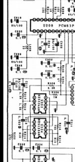
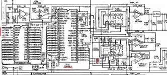
Here I attached an extract from the SM of a Rotel RCD990, with PCM63 + NE5534 as I/V converter.
+ little help with reading the critical path
Attachments
That’s a very good explination. I could not find the impedance of the chip. ThanksArnold,
Yours is a good question.
R2R Dac's are supposed to have high output impedance, though at the end, in practice it's not infinite high, smthing like 1kohm for a PCM63. AD 1862 could be higher though.
A typical opamp I/V converter topology could be also called a Trans Impedance Amplifier, because it absorbs the DAC output current in the -IN feedback node, and converts it into a voltage output with it's transimpedance gain, in this case Rf= 1,5kohm.
Because of the high impedance DAC output the gain is closer to 1 than anything else. So an amp with gain >5 stability criterium will be driven to instability.
But there are ways around it. At the price of accepting a loss at high frequencies, a shunt capacitor to ground placed close to the -IN node of the opamp is presenting a low impedance path at high frequencies in the 'gain' leg of the circuit, which now with the 1,5kohm Rf will give an actual >5 gain factor at high frequencies at re-stabilizing the phase margin.
This is called a 'noise gain compensation' technique for an opamp not unity gain stable.
Here I attached an extract from the SM of a Rotel RCD990, with PCM63 + NE5534 as I/V converter.
+ little help with reading the critical path
AD1862 output impedance can be found from the datasheet: 2.1kohm (+-30%).That’s a very good explination. I could not find the impedance of the chip. Thanks
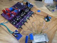
This is quite and dirty functional test, using components on hand (and not by me ") ).
).
Final version will have better components.

And nice & clean 20kHz square wave output, using a functions generator and a resistor to generate input signal current.
No Civ used, just 27R Riv.

Patrick
).Final version will have better components.
And nice & clean 20kHz square wave output, using a functions generator and a resistor to generate input signal current.
No Civ used, just 27R Riv.
Patrick
Hi Guys,
I have an excessive (surprisingly) batch of Genuine Brand-NEW AD1862N that comes directly from DigiKey (Rochester's warehouse, precisely),
only 28pcs in total.
This is a great deal for DIYers that need retail, otherwise you will have to buy at least 14pcs+ plus shipping from Digikey which is surely not a friendly news for individual DIYers.
So you guys might be interested, please go to:
AD1862N 20Bit R2R Ultra Low noise DAC for sale
Last edited:
I always liked the huge packaging of Rochester... particulary not green friendly, lol ! Ah I think Paddy Garcia can have a rest now
you should precise where you are based. It is a great opportuny to someone to make a multichannel 3 ways DAC for active filtering with 3 sets of ad1862 boards with a multichannel USB towards 3 I2S output with uf-l cables to guaranty exact same length on the 3 stereo channels ! DIYHink something is maybe making such an input device perhaps...
you should precise where you are based. It is a great opportuny to someone to make a multichannel 3 ways DAC for active filtering with 3 sets of ad1862 boards with a multichannel USB towards 3 I2S output with uf-l cables to guaranty exact same length on the 3 stereo channels !
DIYHink something is maybe making such an input device perhaps...Thank you for your advice, I have updated the post with shipping costs added.I always liked the huge packaging of Rochester... particulary not green friendly, lol ! Ah I think Paddy Garcia can have a rest now
you should precise where you are based. It is a great opportuny to someone to make a multichannel 3 ways DAC for active filtering with 3 sets of ad1862 boards with a multichannel USB towards 3 I2S output with uf-l cables to guaranty exact same length on the 3 stereo channels !
As stated before, selling these AD1862N is not for profits, it's because something went wrong and I doubled the order
so I have to sell the extra 28pcs of AD1862.So, this is not a regular selling anyway, and hope to help individual DIYers who just need several pcs of AD1862.
| Destination | Tracking Air Pack | |
| USA | 18 | USD |
| Canada | 10 | USD |
| EU | ||
| Germany | 10 | USD |
| France | 10 | USD |
| UK | 10 | USD |
| Norway | 10 | USD |
| Poland | 10 | USD |
| Denmark | 10 | USD |
| Netherlands | 10 | USD |
| Oceania | ||
| Australia | 10 | USD |
| New Zealand | 10 | USD |
| Asia | ||
| Japan | 5 | USD |
| HK | 5 | USD |
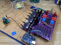
i remove the pins from ic sockets, solder the naked pins on the board.You guys have any recommendations for the best way to "socket" the I/V pins so we can test different resistors in that spot?
Hello @Vunce , you used the following i2s protocols on the JLSounds i2sOverUSB as in post #617?Pulled the DAC board and did another visual inspection, no shorts or solder bridges. I decided to swap out the Singxer C1 USB to I2S converter for JLS I2SoverUSB board configured as in post#617.
Or the i2s protocols as stated in the user manual page 5 under I2S Like Protocols On Board Oscillators for TDA1541?
- Home
- Source & Line
- Digital Line Level
- DAC AD1862: Almost THT, I2S input, NOS, R-2R